
A LED package structure

A technology for LED packaging and LED chips, applied in semiconductor devices, electrical components, circuits, etc., can solve the problems of reduced quantum efficiency of phosphors, unconcentrated light, and scattered light.

Active Publication Date: 2020-07-07
广东安林电子科技股份有限公司
View PDF4 Cites 0 Cited by
  • Summary
  • Abstract
  • Description
  • Claims
  • Application Information

AI Technical Summary

Problems solved by technology

[0003] However, LEDs do not 100% convert electrical energy into light, thus generating a considerable amount of heat. Under the action of high temperature, the colloid encapsulated on the surface of the LED chip is accelerated to age, the luminous efficiency is reduced, and the service life of the LED is greatly reduced. At the same time, The direct contact between the phosphor powder and the LED chip leads to a reduction in the quantum efficiency of the phosphor powder, thereby reducing the light extraction efficiency of the packaging material. In addition, in the prior art, LEDs also have problems such as scattered light emission and non-concentrated light.

Method used


Image

  • A LED package structure
  • A LED package structure
  • A LED package structure

Examples


Embodiment 1

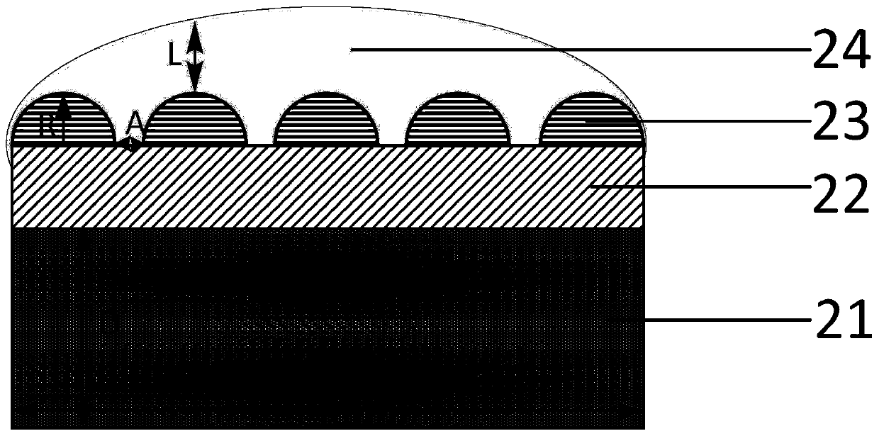
[0036] Such as figure 1 as shown, figure 1 A schematic structural diagram of an LED packaging structure provided by an embodiment of the present invention; wherein, an embodiment of the present invention provides an LED packaging structure, including,

[0037] Heat dissipation substrate 21;

[0038] an LED chip, the LED chip is fixedly connected to the heat dissipation substrate 21;

[0039] The silica gel layer includes a first silica gel layer 22, a hemispherical lens layer 23 and a second silica gel layer 24, the hemispherical lens layer 23 is embedded between the first silica gel layer 22 and the second silica gel layer 24, wherein, The hemispherical lens layer 23 contains a plurality of hemispherical lenses, and the second silica gel layer 24 contains fluorescent powder.

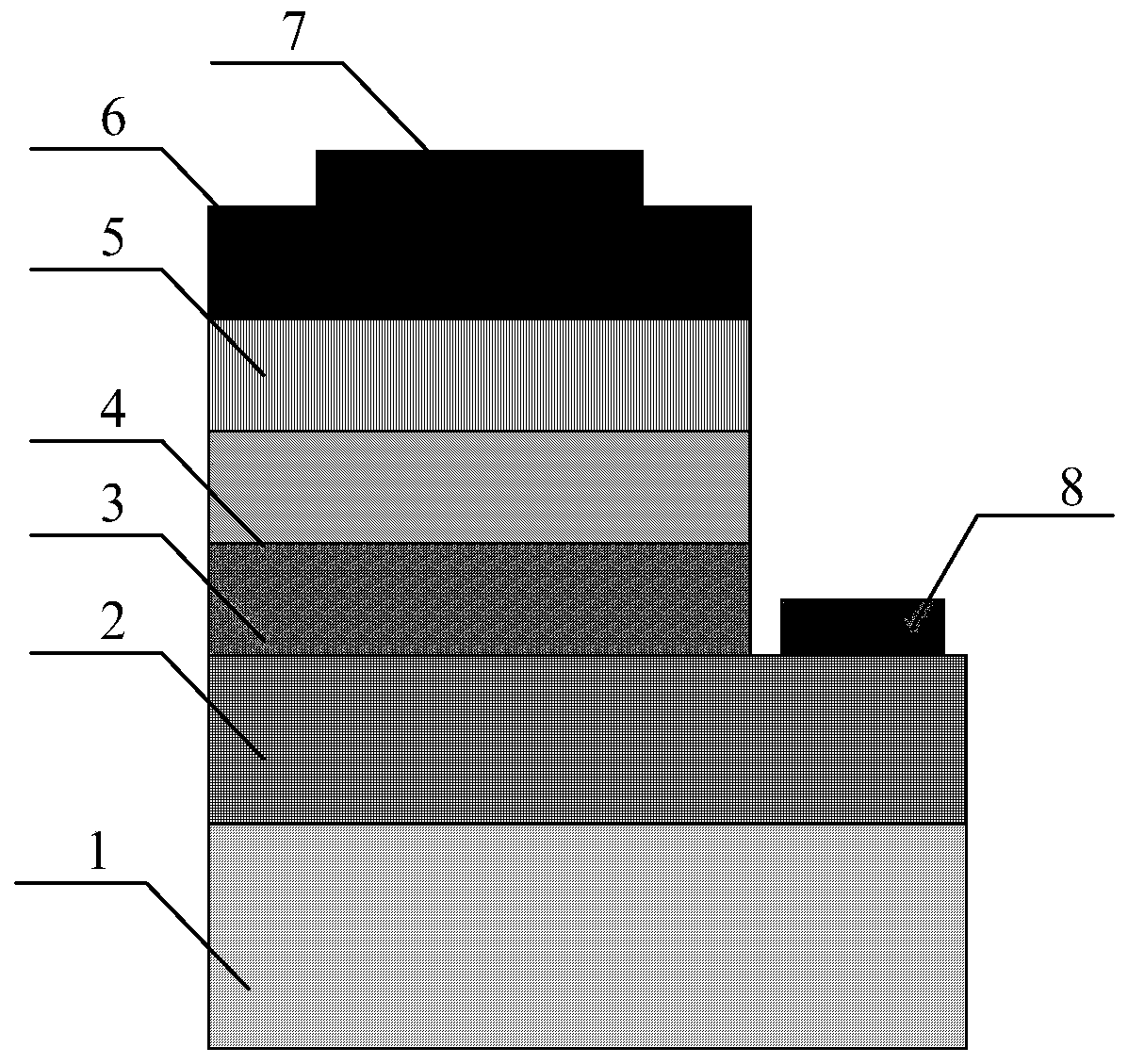
[0040] Such as image 3 as shown, image 3 A schematic structural diagram of an aluminum gallium nitride ultraviolet chip provided by an embodiment of the present invention; the LED chip is an alum...

Embodiment 2

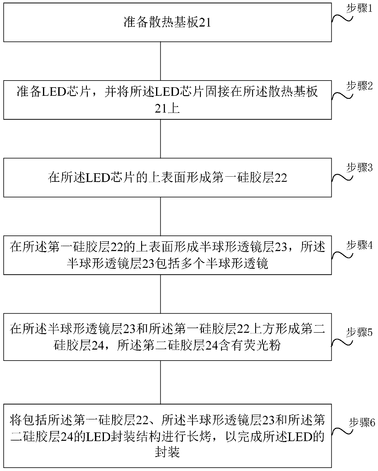
[0055] See figure 2 , figure 2 It is a schematic flowchart of an LED packaging method provided by the embodiment of the present invention; on the basis of the above-mentioned embodiments, this embodiment will introduce the process flow of the present invention in more detail. The method includes:

[0056] Step 1, preparing the heat dissipation substrate 21;

[0057] Specifically include: selecting the heat dissipation substrate 21;

[0058] Clean the heat dissipation substrate 21, and clean the stains on the heat dissipation substrate 21, especially the oil stains;

[0059] The heat dissipation substrate 21 is dried.

[0060] Step 2, preparing LED chips, and fixing the LED chips on the heat dissipation substrate 21;

[0061] In the embodiment of the present invention, the LED chip is an aluminum gallium nitride ultraviolet chip (AlGaN), such as image 3 as shown, image 3 The structural schematic diagram of the LED chip in the LED packaging structure provided by the emb...

Embodiment 3

[0082] Please combine figure 1 , Figure 4 as well as Figure 5A and Figure 5B as shown, figure 1 A schematic structural diagram of an LED packaging structure provided by an embodiment of the present invention; Figure 4 It is a schematic diagram of the light emitting principle of an LED packaging structure provided by an embodiment of the present invention; Figure 5A , Figure 5B It is a schematic diagram of an arrangement of a plurality of hemispherical lenses provided by an embodiment of the present invention.

[0083] Such as figure 1 As shown, the LED packaging structure provided by the embodiment of the present invention includes

[0084] Heat dissipation substrate 21;

[0085] an LED chip, the LED chip is fixedly connected to the heat dissipation substrate 21;

[0086] The silica gel layer includes a first silica gel layer 22, a hemispherical lens layer 23 and a second silica gel layer 24, the hemispherical lens layer 23 is embedded between the first silica g...


PUM

PropertyMeasurementUnit
diameteraaaaaaaaaa
thicknessaaaaaaaaaa
refractive indexaaaaaaaaaa

Abstract

The invention relates to an LED packaging structure, which comprises a heat dissipation substrate (21), an LED chip and a silica gel layer, wherein the LED chip is fixedly connected to the heat dissipation substrate (21); the silica gel layer comprises a first silica gel layer (22), a hemispherical lens layer (23) and a second silica gel layer (24); the hemispherical lens layer (23) is embedded between the first silica gel layer (22) and the second silica gel layer (24); the hemispherical lens layer (23) comprises a plurality of hemispherical lenses; and the second silica gel layer (24) contains fluorescent powder. According to the LED packaging structure, the hemispherical lens layer is arranged between the first silica gel layer and the second silica gel layer, and the fluorescent powderis contained in the second silica gel layer, so that light beams are more concentrated and uniform in irradiation, direct contact of the fluorescent powder and the LED chip is avoided and the light extraction efficiency is improved.

Description

technical field [0001] The invention belongs to the technical field of photoelectric devices, and in particular relates to an LED packaging structure. Background technique [0002] An LED is a semiconductor that produces light of various colors when a voltage is applied. The color of light produced by each LED typically depends on the chemical composition of the LED chip and phosphor. The demand for LED continues to grow because it has various advantages compared with lighting devices using filaments, such as its high tolerance to frequent power switching, high vibration resistance, long life, low driving voltage, excellent Startup features. [0003] However, LEDs do not 100% convert electrical energy into light, thus generating a considerable amount of heat. Under the action of high temperature, the colloid encapsulated on the surface of the LED chip is accelerated to age, the luminous efficiency is reduced, and the service life of the LED is greatly reduced. At the same ...

Claims


Application Information

Patent Timeline
Patent Type & Authority Patents(China)
IPC IPC(8): H01L33/50H01L33/56H01L33/58
CPCH01L33/504H01L33/507H01L33/56H01L33/58
Inventor 张亮
Owner 广东安林电子科技股份有限公司
Learn More