Array substrate and organic luminescent display panel

An array substrate, one-sided technology, used in electrical components, electrical solid devices, circuits, etc., can solve the problem of easy cracking of metal wires, and achieve the effect of solving easy cracking and increasing the length of lines

Active Publication Date: 2018-05-11
EVERDISPLAY OPTRONICS (SHANGHAI) CO LTD
View PDF7 Cites 24 Cited by
  • Summary
  • Abstract
  • Description
  • Claims
  • Application Information

AI Technical Summary

Problems solved by technology

[0004] Embodiments of the present invention provide an array substrate and an organic light-emitting display panel to solve the problem that the metal wires of the existing AMOLED are easy to crack when bent

Method used


Image

  • Array substrate and organic luminescent display panel
  • Array substrate and organic luminescent display panel
  • Array substrate and organic luminescent display panel

Examples


Embodiment Construction

[0038] In order to make the purpose, technical solutions and advantages of the present invention clearer, the technical solutions of the present invention will be clearly and completely described through implementation with reference to the accompanying drawings in the embodiments of the present invention. Obviously, the described embodiments are the embodiment of the present invention. Some, but not all, embodiments. Based on the embodiments of the present invention, all other embodiments obtained by persons of ordinary skill in the art without making creative efforts belong to the protection scope of the present invention.

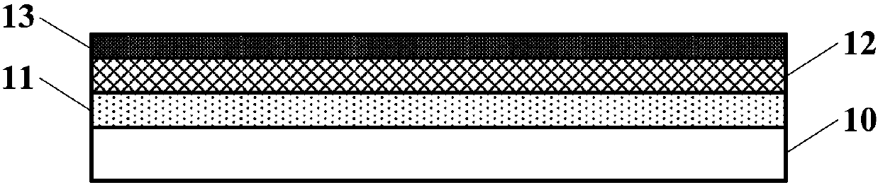
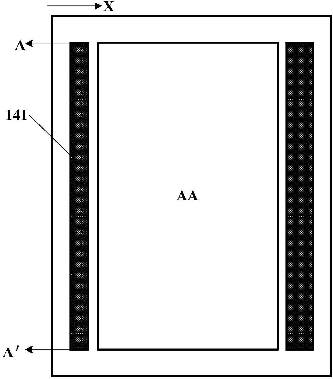
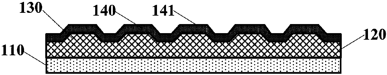
[0039] Such as Figure 2A , which is a schematic diagram of an array substrate provided in Embodiment 1 of the present invention, Figure 2B yes Figure 2A Sectional view along A-A'. The array substrate of this embodiment is suitable for an organic light emitting display panel. The array substrate provided in this embodiment includes: a substrate 110...


PUM

PropertyMeasurementUnit
thicknessaaaaaaaaaa
densityaaaaaaaaaa
thicknessaaaaaaaaaa

Abstract

The invention discloses an array substrate and an organic luminescent display panel. The array substrate comprises a substrate, an inorganic insulation layer positioned on the substrate, and a metal line layer positioned on the side, far from the substrate, of the inorganic insulation layer. The side, far from the substrate, of the inorganic insulation layer includes multiple projection structures, the metal line layer extends along the projection structures in a climbing way, and the extension length of the metal line layer can be increased substantially via arrangement of the projection structures. Compared with the prior art, the extension length of the metal line layer in the bending direction is increased in the array substrate, the bending radii of the metal line layer is lower, themetal line layer can bear a lower bending radii and is not cracked, and the problem that a metal line is easy to crack during bending in the prior art is solved.

Description

technical field [0001] Embodiments of the present invention relate to flexible panel technology, and in particular to an array substrate and an organic light emitting display panel. Background technique [0002] Active matrix OLED (AMOLED) is a self-luminous display device. AMOLED has better picture quality than liquid crystal display. AMOLED is also a thin-film solid-state device, so this makes it easier to use for flexible displays. [0003] Such as figure 1 Shown is a partial structural diagram of an existing flexible AMOLED, including a glass substrate 10 , a flexible PI film 11 , an inorganic film layer 12 and metal wires 13 . When the flexible AMOLED is bent, the inorganic film layer 12 is prone to rupture due to its internal stress and density, and the corresponding metal wiring 13 on the inorganic film layer 12 may also be broken or disconnected. In addition, the fracture strain limit of the metal itself is about 1%. When the flexible AMOLED is bent, the extension ...

Claims


Application Information

Patent Timeline
Patent Type & Authority Applications(China)
IPC IPC(8): H01L27/32
CPCH10K59/131
Inventor 盛晨航李园园
Owner EVERDISPLAY OPTRONICS (SHANGHAI) CO LTD
Why Eureka
Try Eureka