Nonvolatile memory chip capable of being automatically subjected to physical destruction

A non-volatile storage and physical destruction technology, applied in the field of non-volatile memory chips, can solve the problems of high cost, slow destruction speed, large device size, etc., and achieve the effect of low power consumption, fast speed, and non-recoverable power consumption

Pending Publication Date: 2018-06-05
HONGQIN (BEIJING) TECHNOLOGY CO LTD
View PDF4 Cites 1 Cited by
  • Summary
  • Abstract
  • Description
  • Claims
  • Application Information

AI Technical Summary

Problems solved by technology

[0003] The present invention aims at the shortcomings of the existing methods, such as large volume, high cost, slow destruction speed, and the destruction effect is limited by

Method used


Image

  • Nonvolatile memory chip capable of being automatically subjected to physical destruction

Examples


Embodiment 1

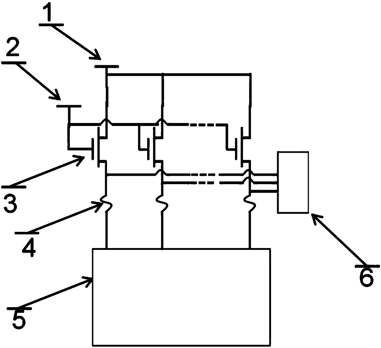
[0019] A non-volatile memory chip capable of self-physical destruction, a non-volatile memory chip capable of self-physical destruction, the non-volatile memory chip includes a packaging device and a chip device, and the chip device includes several groups of fuse units , a data unit, and a fuse control unit; the fuse unit is arranged on the data unit; the fuse control unit and the fuse unit are connected in series; and the packaging device is arranged outside the chip device. The packaging device is a package of rectangular sheets, and the package includes a cavity and pins. The fuse unit includes a metal fuse 4 and a fuse power supply; the number of the metal fuse 4 is 36. The fuse control unit includes a fuse switch and a fuse switch control power supply 2 . The fuse switch is a transistor 3 . The voltage of the fuse switch control power supply is 3V. The data unit includes a non-volatile storage array 5 and a storage read-write circuit 6 . The fuse unit is connected in...


PUM


Abstract

The invention provides a nonvolatile memory chip capable of being automatically subjected to physical destruction. The nonvolatile memory chip comprises a packaging device and a chip device, wherein the chip device comprises multiple groups of fusion units, a data unit and a fusion control unit; each group of fusion units is arranged on the data unit; the fusion control unit and the fusion units are connected in series; each group of fusion unit comprises a metal fuse wire and a fusion power supply, and all fusion power supplies are connected in parallel; each group of fusion control units comprises a fusion switching control power supply, and all fusion switching control power supplies are connected in parallel; and the packaging device is arranged out of the chip device. When the way isadopted to destroy chips, speed is high, power consumption is low, and the chip can not be recovered.

Description

technical field [0001] The invention relates to the technical field of chip destruction, in particular to a nonvolatile memory chip capable of self-physical destruction. Background technique [0002] Data security is very important in special fields such as finance and national defense. In some specific cases, key data leakage can be avoided by physically destroying the data storage chip and control chip on the electronic storage carrier to make the data stored on it completely unreadable. . At present, the existing physical destruction method is to take power from the destruction device directly from the working power supply of the storage device (such as solid-state electronic hard disk, U disk, etc.), and directly and continuously load the destruction power of high voltage and high current to the chip to be destroyed , until the destroyed chip cannot withstand the continuous power input of high voltage and high current, which causes the ablation of the wiring and the die...

Claims


Application Information

Patent Timeline
IPC IPC(8): G11C17/16G06F21/78
CPCG06F21/78G11C17/16
Inventor 吕景成杨建利张涛周洋
Owner HONGQIN (BEIJING) TECHNOLOGY CO LTD
Why Eureka
Try Eureka