Manufacturing method of curved frequency selective surface array

A technology of frequency selective surface and fabrication method, applied in the direction of electrical components, antennas, etc., can solve the problem of inability to fabricate a patch-type FSS curved surface unit array, etc., and achieve the effect of strong versatility and good matching.

Active Publication Date: 2018-06-05
CHANGCHUN INST OF OPTICS FINE MECHANICS & PHYSICS CHINESE ACAD OF SCI
View PDF4 Cites 11 Cited by
  • Summary
  • Abstract
  • Description
  • Claims
  • Application Information

AI Technical Summary

Benefits of technology

This patented technology allows for creation of curled fused silicon (FSC) structures without being restricted from their complicated geometry or requiring expensive equipment like lithography techniques. It also enables production of various types of FSFAs such as microstrip lines, strips, spiral waveguides, etc., while maintaining flexibility over large areas. Additionally, it provides an improved way to make these materials on different surfaces through direct printing processes instead of traditional photolithographic pattern formation steps. Overall, this process offers technical benefits including increased efficiency, customization options, reduced costs associated therewith, enhanced performance capabilities, and easier implementation across multiple industries' needs.

Problems solved by technology

This patented technical problem addressed in this patents relates to improving the design flexibility and applicability of FSS surfaces due to their ability to filter out unwanted signals from targets without affecting their operation or functionality. Current methods require complicated processes like lamination onto flat substrate layers, thermal plasma spray coating, laser etching, solvent casting, electroforming, mechanical milling, molding, welding, bonding, gluing, and others, making them difficult to apply within specific types of target curvatures.

Method used


Image

  • Manufacturing method of curved frequency selective surface array
  • Manufacturing method of curved frequency selective surface array
  • Manufacturing method of curved frequency selective surface array

Examples


Embodiment 1

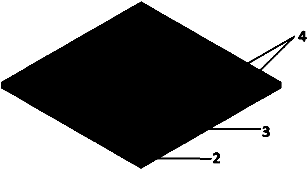
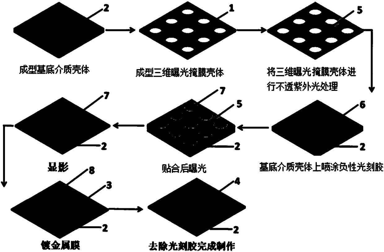
[0056] In this embodiment, a circular opening type (referred to as round hole) curved surface FSS array is formed on the above-mentioned base dielectric shell 2, such as figure 2 As shown, a metal layer 3 is attached to the base dielectric shell 2, and an array of circular hole units 4 is formed on the metal layer 3. The main manufacturing process is as follows image 3 As shown, it specifically includes the following steps:

[0057] (1) The three-dimensional exposure mask housing 1 is modeled with Solidworks software, and the three-dimensional exposure mask housing 1 is distributed with hollow circular holes, the size of which is consistent with the size of the finally formed circular hole unit 4; the three-dimensional exposure mask The shell 1 and the outer surface of the base dielectric shell 2 are shaped, and the thickness of the three-dimensional exposure mask shell 1 in this embodiment is 0.5mm;

[0058] (2) The photosensitive resin is used as the raw material, and the...

Embodiment 2

[0066] In this embodiment, a circular patch type (circular patch for short) FSS array is formed on the above-mentioned base dielectric shell 2, as Figure 4 As shown, an array of circular patch units 9 is prepared on the substrate dielectric shell 2, and the main process flow is as follows Figure 5 As shown, it specifically includes the following steps:

[0067] (1) Modeling the three-dimensional exposure mask housing 1 with Solidworks software, the three-dimensional exposure mask housing 1 is distributed with hollow circular holes, and the size of the circular holes is consistent with the size of the finally formed circular patch unit 9; the three-dimensional exposure mask The outer surface of the film case 1 and the base dielectric case 2 is shaped, and the thickness of the three-dimensional exposure mask case 1 in this embodiment is 0.5 mm;

[0068] (2) The photosensitive resin is used as the raw material, and the mask shell is printed by the stereolithography (SLA) proce...


PUM

PropertyMeasurementUnit
Thicknessaaaaaaaaaa
Thicknessaaaaaaaaaa
Thicknessaaaaaaaaaa

Abstract

The invention relates to the technical field of FSS (Frequency Selective Surface) radome manufacturing, and specifically discloses a manufacturing method of a curved frequency selective surface array.The manufacturing method comprises the steps of S1, respectively performing three-dimensional modeling on a substrate dielectric shell and a three-dimensional exposure mask shell through three-dimensional modeling software; S2, respectively inputting a substrate dielectric shell model and a three-dimensional exposure mask shell module into 3D printing equipment for molding; S3, coating the outersurface of the substrate dielectric shell with a photoresist, attaching the three-dimensional exposure mask shell to the molded substrate dielectric shell, enabling the two layers to be tightly laminated, and performing exposure processing through exposure equipment; S4, performing development processing, cleaning and drying on the substrate dielectric shell; and S5, preparing a metal film layer on the surface of the processed substrate dielectric shell, and removing the left photoresist by using a photoresist removing liquid, cleaning and drying. The manufacturing method not only can manufacture a hole unit array, but also can manufacture a patch unit array, and has good universality.

Description


Claims


Application Information

Patent Timeline
Owner CHANGCHUN INST OF OPTICS FINE MECHANICS & PHYSICS CHINESE ACAD OF SCI
Why Eureka
Try Eureka