Flexible display screen and manufacturing method thereof
A technology for flexible display screens and manufacturing methods, applied to identification devices, instruments, etc., can solve problems such as lower yield rate, loose FPC binding, abnormal display, etc., to reduce the number of bending times, avoid film layer breakage, and avoid bending The effect of too small a radius
- Summary
- Abstract
- Description
- Claims
- Application Information
AI Technical Summary
Problems solved by technology
Method used
Image
Examples
Embodiment 1
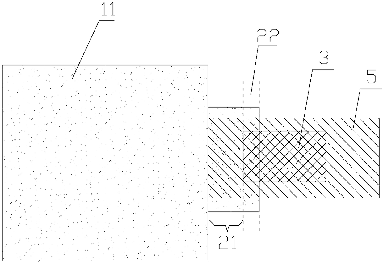
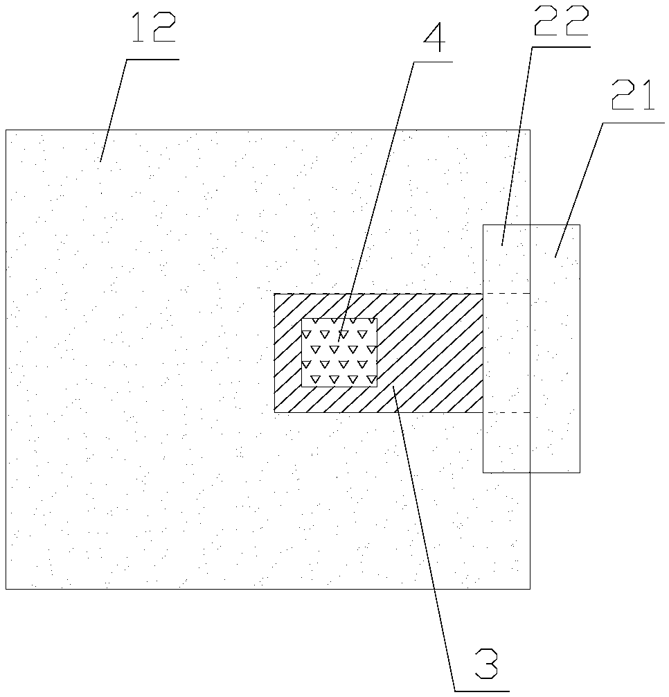
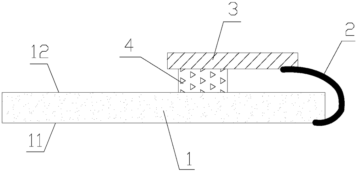
[0042] This embodiment provides a flexible display screen 1, which can be referred to Figure 1 ~ Figure 3 As shown, it includes a front 11 for display and a back 12 provided with a circuit board, a display area is set on the front 11, and the flexible display 1 also includes:
[0043] Outer Lead Bonding (OLB for short) zone 2, connected to the end of the front surface 11;
[0044] The binding area 22 is set on the outer lead welding area 2;
[0045] The bending part 21 is arranged on the outer lead welding area 2, and is located in the display area (the display area basically covers the area of the front 11 except the edge, so the front 11 can be regarded as the display area equivalently in the figure) and the binding between zone 22;
[0046] A flexible printed circuit (FPC for short) 3 is fixed on the binding area 22;
[0047] The supporting member 4 is arranged on the back surface 12 of the flexible display screen 1;
[0048] Wherein, the flexible circuit board 3 is ...
Embodiment 2
[0052] This embodiment provides a method for manufacturing a flexible display screen, referring to Figure 1 ~ Figure 3 As shown, the flexible display screen 1 includes a front side 11 for display and a back side 12 provided with a circuit board, and a display area is arranged on the front side 11. After the glass substrate is removed from the mold, the flexible display is bent; the specific manufacturing method includes:
[0053] Provide an outer lead welding area 2, which is arranged at the end of the front surface 11;
[0054] Provide a binding area 22, set on the outer lead welding area 2;
[0055] A bending portion 21 is provided, which is arranged on the outer lead welding area 2, and is located between the binding area 22 and the display area (the display area basically covers the area of the front side 11 except the edge, so the front side 11 can be viewed equivalently in the figure. for the display area);
[0056] Provide a flexible circuit board 3, fixed on the ...
PUM
 Abstract
Description
Claims
Application Information


