
Pixel compensation circuit and aging method thereof

A technology for compensating circuits and pixels, applied to instruments, static indicators, etc., can solve problems such as uneven product display, increased TFT leakage current, and bright spots

Inactive Publication Date: 2018-07-17
TRULY HUIZHOU SMART DISPLAY
View PDF5 Cites 15 Cited by
  • Summary
  • Abstract
  • Description
  • Claims
  • Application Information

AI Technical Summary

Problems solved by technology

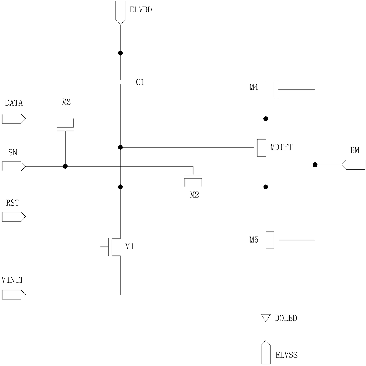
[0006] Based on this, it is necessary to address the space compression due to the improvement of the existing TFT precision, resulting in the change of the width and length of the TFT, and with the decrease of the line width, the leakage current of the TFT increases, resulting in poor display of the product. To solve the technical problem of uniform or bright spots, a pixel compensation circuit and its aging method are provided

Method used

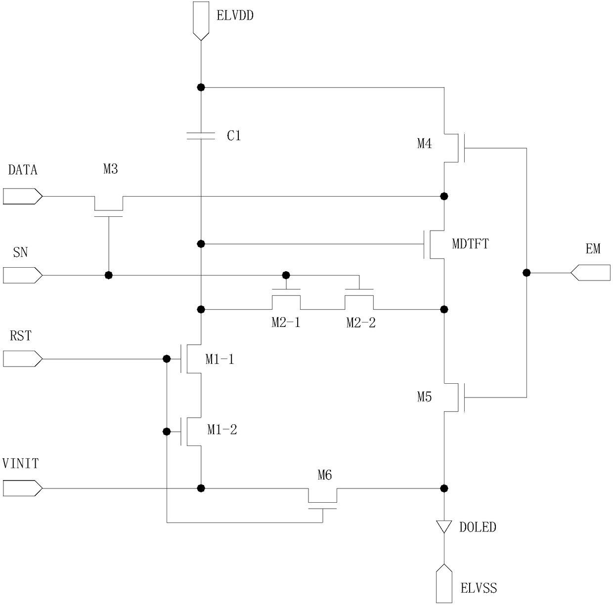
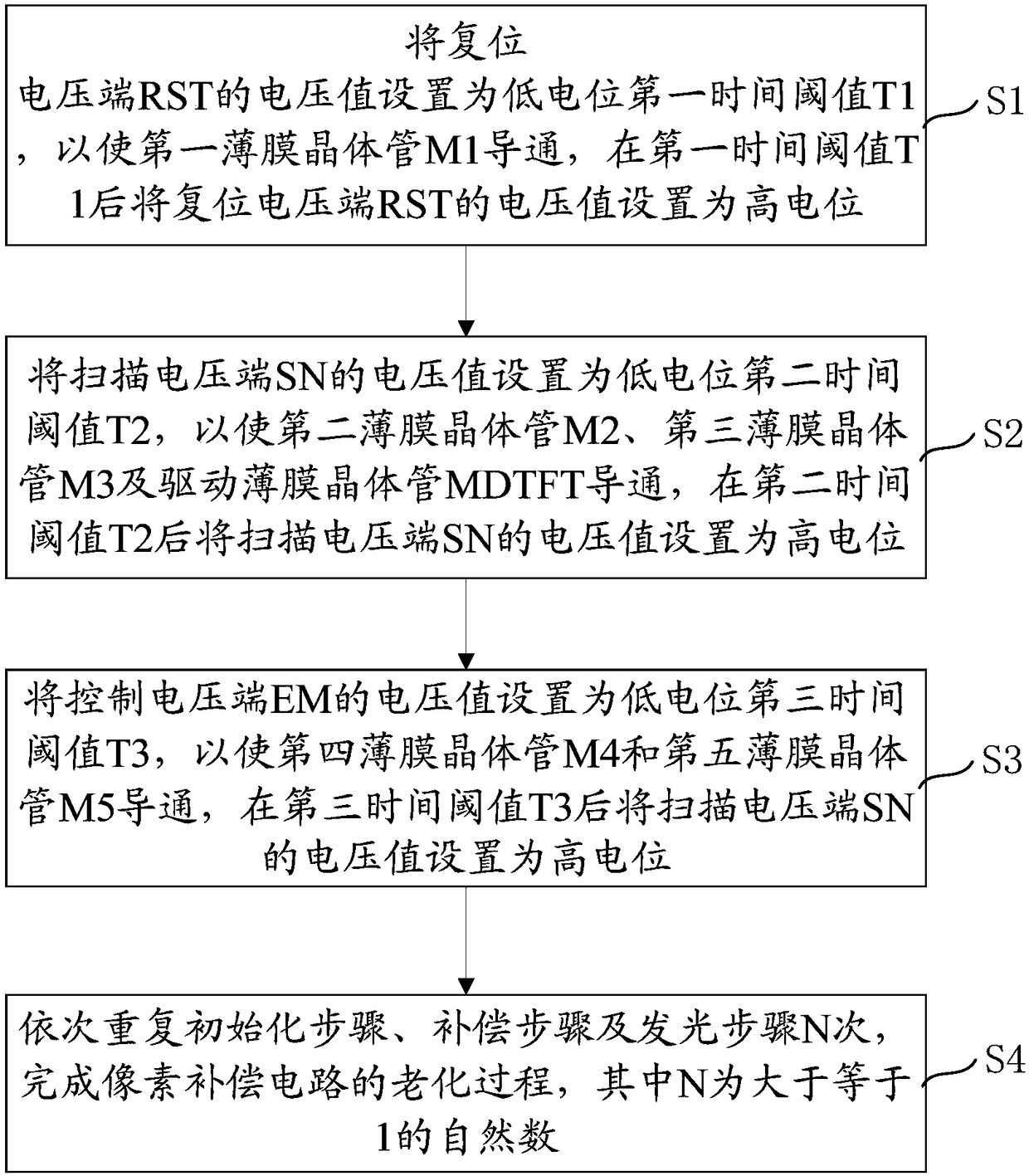

Image

  • Pixel compensation circuit and aging method thereof
  • Pixel compensation circuit and aging method thereof
  • Pixel compensation circuit and aging method thereof

Examples


Embodiment Construction

[0026] In order to make the above objects, features and advantages of the present invention more comprehensible, specific implementations of the present invention will be described in detail below in conjunction with the accompanying drawings. In the following description, numerous specific details are set forth in order to provide a thorough understanding of the present invention. However, the present invention can be implemented in many other ways different from those described here, and those skilled in the art can make similar improvements without departing from the connotation of the present invention, so the present invention is not limited by the specific embodiments disclosed below.

[0027] In addition, the terms "first" and "second" are used for descriptive purposes only, and cannot be interpreted as indicating or implying relative importance or implicitly specifying the quantity of indicated technical features. Thus, the features defined as "first" and "second" may ...


PUM


Abstract

A pixel compensation circuit and an aging method thereof are disclosed. The pixel compensation circuit comprises a first thin film transistor, a second thin film transistor, a third thin film transistor, a fourth thin film transistor, a fifth thin film transistor, a driving thin film transistor, a capacitor, a luminous diode, a reset voltage end, an initial voltage end, a first voltage source end,a scanning voltage end, a data voltage end, a control voltage end and a second voltage source end, wherein the voltage value of the initial voltage end is greater than that of the first voltage source end, the voltage value of the data voltage end is greater than that of the initial voltage end, and the voltage value of the first voltage source end is greater than that of the second voltage source end. The pixel compensation circuit and the aging method rearrange the defective electrons of the drive thin film transistor MDTFT channel and interface in an abnormal working state by driving the reverse bias of the thin film transistor, thereby reducing the leakage current of the drive thin film transistor.

Description

technical field [0001] The invention relates to the field of display technology, in particular to a pixel compensation circuit and an aging method thereof. Background technique [0002] AMOLED (Active-matrix organic light emitting diode, active-matrix organic light-emitting diode) display screen has been favored by the panel preparation industry and mobile phone, Computer and other manufacturers of widespread concern. [0003] With the development of science and technology, in the market development trend of display products, the resolution of display products will become higher and higher. With the improvement of product resolution, the manufacturing process and preparation difficulty of LTPS (Low Temperature Poly-silicon, low temperature polysilicon technology) backplane will become more and more difficult, and various TFT (Thin Film Transistor, thin film transistor) also need more and more Making it smaller will damage some of the performance of the product. [0004] C...

Claims


Application Information

Patent Timeline
Patent Type & Authority Applications(China)
IPC IPC(8): G09G3/3225
CPCG09G3/3225G09G2320/0233
Inventor 刘世奇任思雨苏君海李建华
Owner TRULY HUIZHOU SMART DISPLAY
Learn More