Method for uniformity analysis of superconducting nanowire based on elemental imaging
A technology of superconducting nanowires and uniformity, which is applied in the fields of analyzing materials, material analysis using wave/particle radiation, measuring devices, etc., which can solve problems such as difficulty in screening in the early stage
- Summary
- Abstract
- Description
- Claims
- Application Information
AI Technical Summary
Problems solved by technology
Method used
Image

Examples
Embodiment
[0023] Embodiment: this embodiment comprises the following steps:
[0024] (1) Superconducting nanowire sample preparation
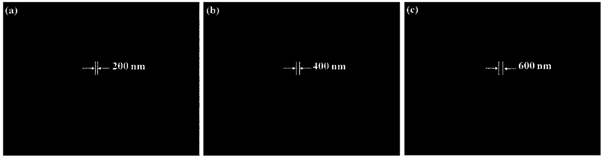
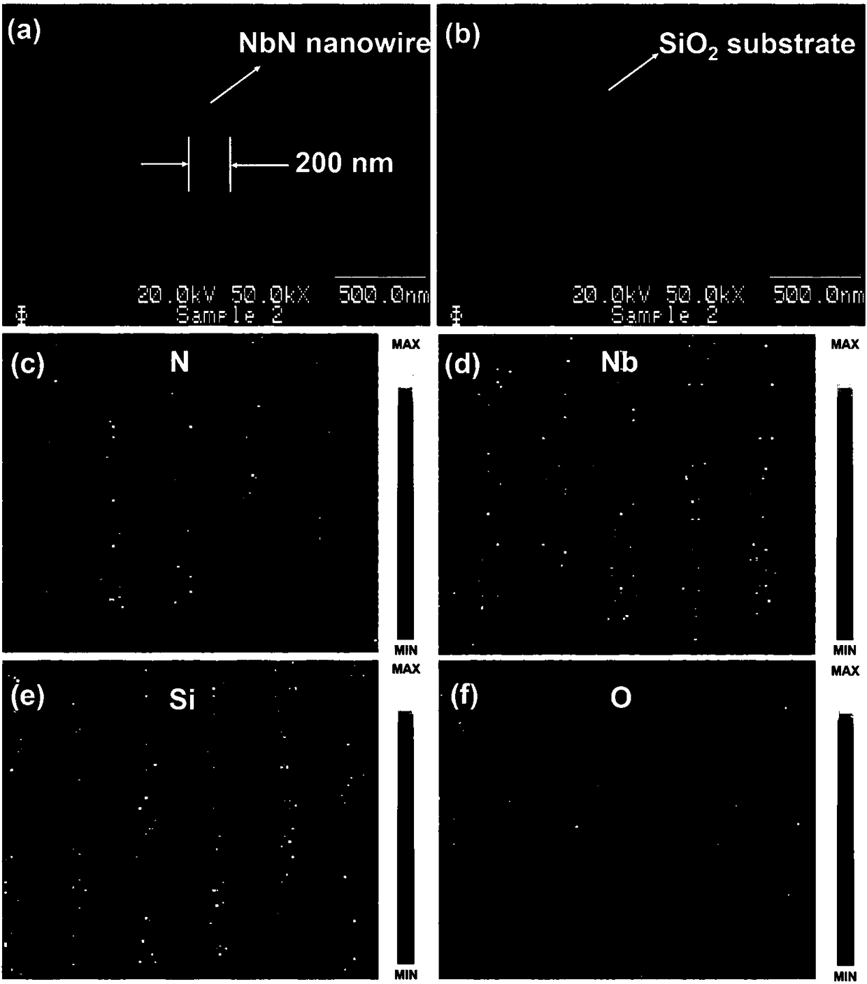
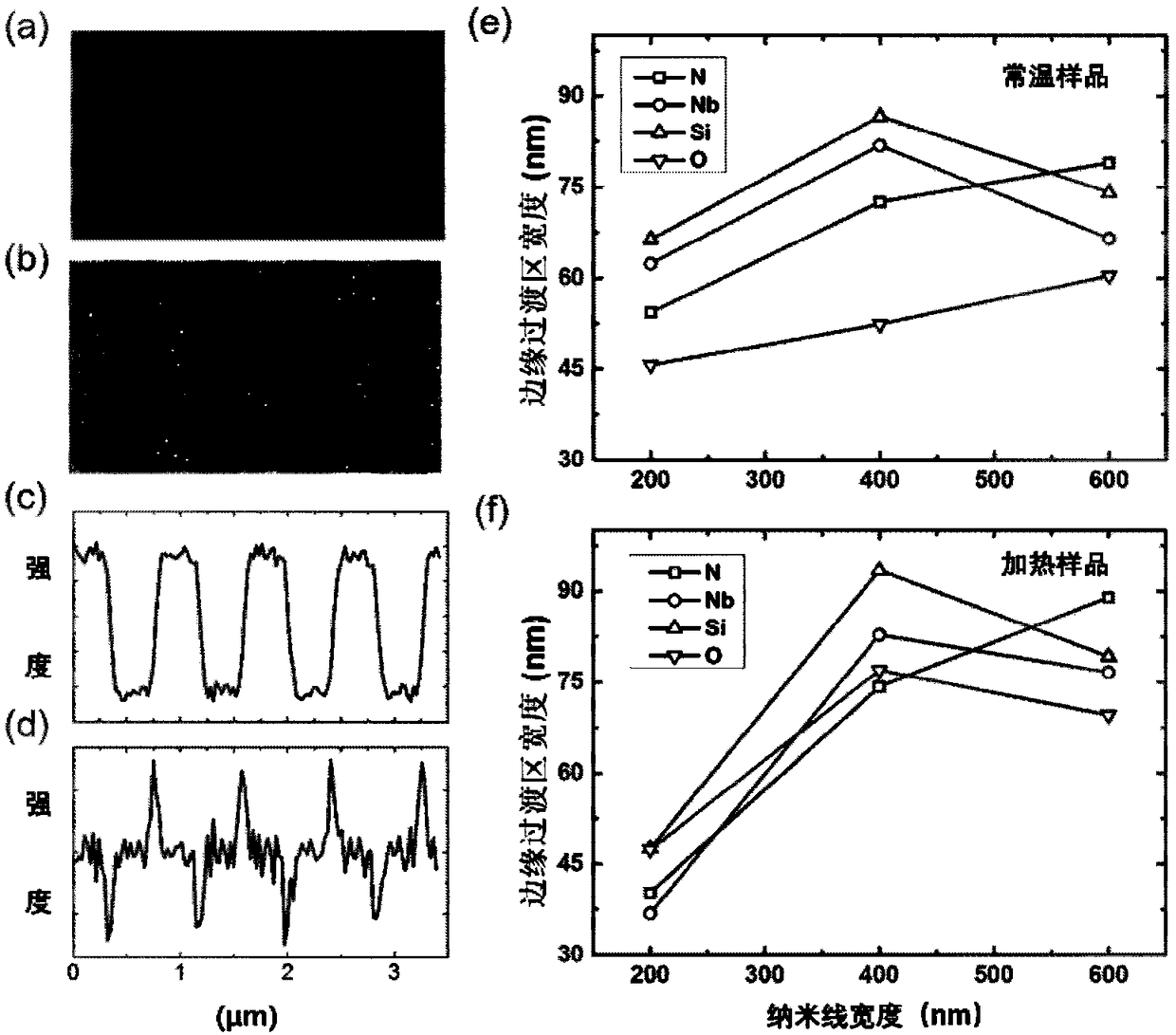
[0025] Select a 6nm thick NbN film prepared under normal temperature and heating conditions, use the same conditions for electron beam etching (EBL), and use Ar / SF6 gas for reactive ion etching (RIE) to obtain the same shape and line width of 200nm , 400nm, 600nm nanowire meander structure, the sample size is 12*18μm2, figure 1 Scanning electron microscope images of nanowires of different linewidths are given.
[0026] (2) AES element imaging
[0027] Scanning elemental imaging of the nanowire region was performed using Auger Electron Spectroscopy (AES).
[0028] Raw data were obtained using Auger electron spectroscopy because it is a surface-sensitive analytical technique that utilizes a beam of high-energy electrons as an excitation source. The kinetic energy of Auger electrons reflects the characteristic information of the currently detected eleme...
PUM
 Abstract
Description
Claims
Application Information
 - R&D
- Intellectual Property
- Life Sciences
- Materials
- Tech Scout
- Unparalleled Data Quality
- Higher Quality Content
- 60% Fewer Hallucinations
Browse by: Latest US Patents, China's latest patents, Technical Efficacy Thesaurus, Application Domain, Technology Topic, Popular Technical Reports.
© 2025 PatSnap. All rights reserved.Legal|Privacy policy|Modern Slavery Act Transparency Statement|Sitemap|About US| Contact US: help@patsnap.com