Minority carrier lifetime detection device and detection method
What is AI technical title?
AI technical title is built by Patsnap AI team. It summarizes the technical point description of the patent document.
A minority carrier lifetime and detection method technology, applied in the field of semiconductors, can solve the problems of inability to truly reflect the performance of semiconductor materials and low accuracy
Active Publication Date: 2018-10-19
YUNGU GUAN TECH CO LTD
View PDF7 Cites 0 Cited by
Summary
Abstract
Description
Claims
Application Information
AI Technical Summary
This helps you quickly interpret patents by identifying the three key elements:
Problems solved by technology
Method used
Benefits of technology
Problems solved by technology
Therefore, the traditional test method of minority carrier lifetime measured according to the change trend of electrical conductivity over time has low accuracy and cannot truly reflect the performance of semiconductor materials.
Method used
Image
Click on the blue label to locate the original text in one second.
Reading with bidirectional positioning of images and text.
Examples
Embodiment 1
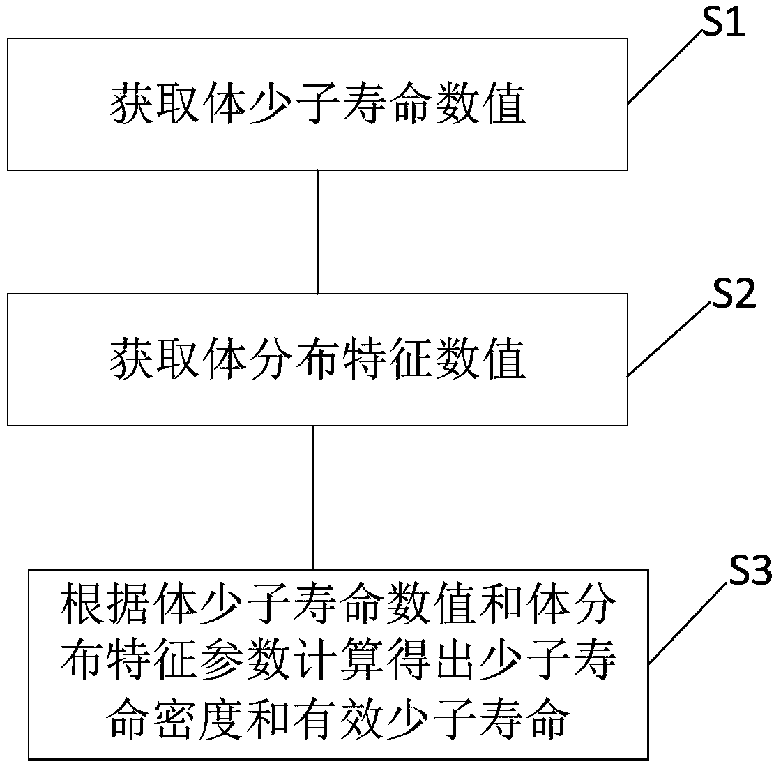
[0066] This embodiment provides a detection method for the minority carrier lifetime, such as figure 1 shown, including the following steps:
[0067] Step S1, obtaining the value of the lifespan of the low-body population;
[0068] Step S2, obtaining volume distribution characteristic parameters;
[0069] Step S3, calculating the minority carrier lifetime density and the effective minority carrier lifetime according to the numerical value of the bulk minority carrier lifetime and the characteristic parameters of the volume distribution.
[0070] As an implementation manner of this embodiment, step S1 specifically includes the following steps:
[0071] Step S11, using an external light source to irradiate the surface of the object to be tested; in this embodiment, the object to be tested is a semiconductor layer, selected from but not limited to any one of amorphous silicon material, polysilicon material, metaloxide semiconductor material, etc., through An external light so...
Embodiment 2
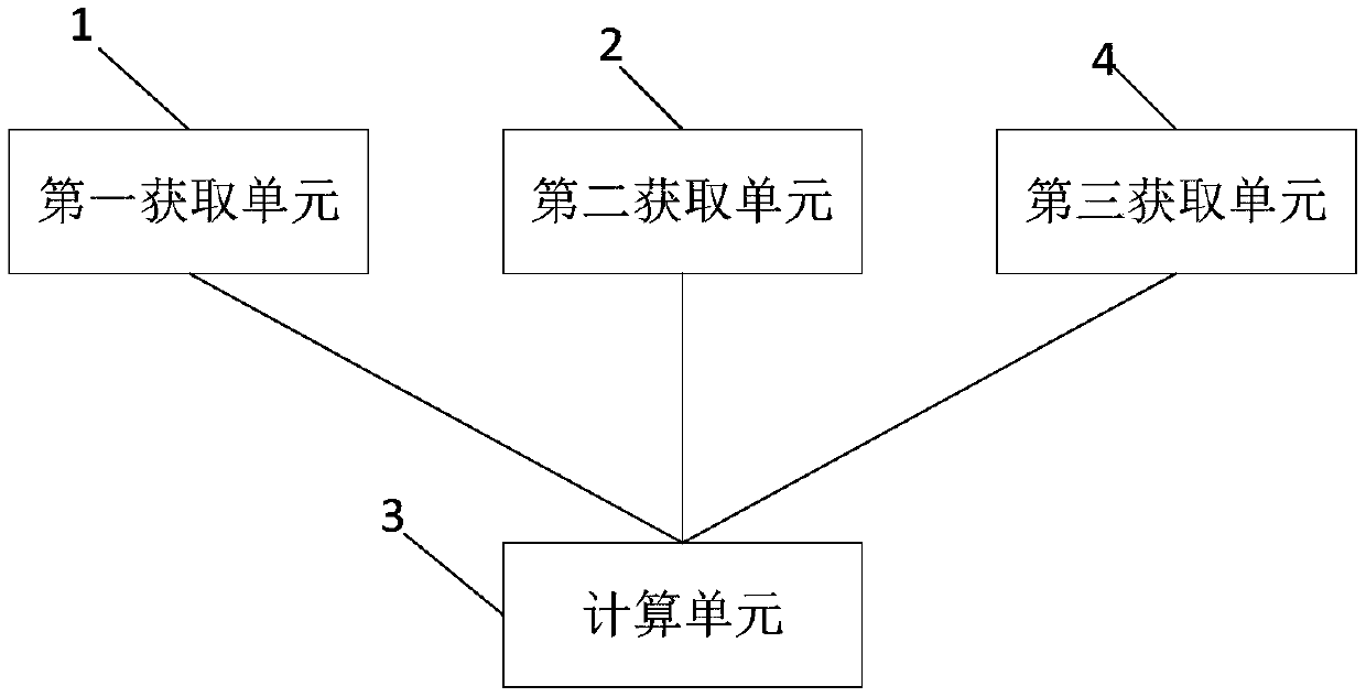
[0105] This embodiment provides a minority carrier lifetime detection device, including a first acquisition unit 1, a second acquisition unit 2, and a calculation unit 3, wherein:
[0106] The first acquisition unit 1 is used to acquire the value of body minority lifetime;
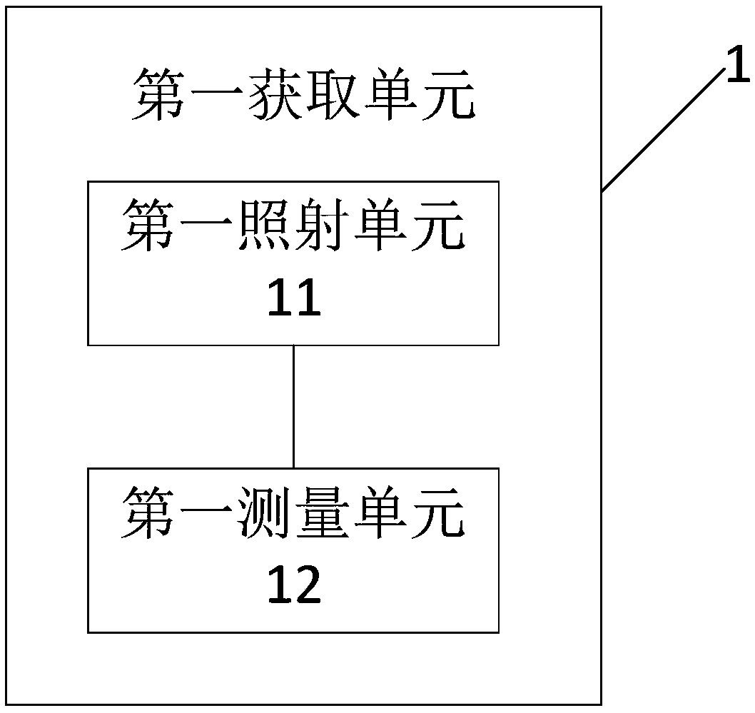
[0107] In this embodiment, the first acquisition unit 1 includes a first irradiation unit 11 and a first measurement unit 12, wherein:
[0108] The first irradiation unit 11 is used to irradiate the surface of the object to be tested with an external light source. In this embodiment, the object to be tested is a semiconductor layer, which is selected from but not limited to amorphous silicon material, polysilicon material, metaloxide semiconductor material, etc. One, the external light source is selected from but not limited to any one of ultraviolet light source, laser light source and other light sources, the selected external light source is determined according to the material of the object to be test...
PUM
Abstract
The invention relates to the technical field of semiconductors, and discloses a minority carrier lifetime detection method comprising the steps that the body minority carrier lifetime value is acquired; the body distribution characteristic parameters are acquired; and the minority carrier lifetime density and the effective minority carrier lifetime are obtained according to the body minority carrier lifetime value and the body distribution characteristic parameters. The body minority carrier lifetime value is acquired and the semiconductor layer body distribution characteristic parameters arealso acquired, and the minority carrier lifetime density and the effective minority carrier lifetime are obtained through combination of the body minority carrier lifetime value and the body distribution characteristic parameters so that the detection method has high accuracy and can truly reflect the minority carrier lifetime and the performance of the semiconductor layer material.
Description
technical field [0001] The invention relates to the technical field of semiconductors, in particular to a minority carrier lifetime detection device and detection method. Background technique [0002] With the vigorous development of the high-tech industry represented by the microelectronics industry, the research, development and application of semiconductor materials have become an important direction of priority development in the industrial field. In the research of semiconductor materials, the lifetime of minority carriers (minority carriers) is directly related to the performance of semiconductor devices, and is one of the important parameters of semiconductor materials. [0003] Most of the existing methods for measuring the minority carrier lifetime are based on the principle of photoconductive decay, including two processes of electron-hole generation by light injection and change of microwave detection signal. The specific measurement principle is: laser injection...
Claims
Application Information
Patent Timeline
Application Date:The date an application was filed.
Publication Date:The date a patent or application was officially published.
First Publication Date:The earliest publication date of a patent with the same application number.
Issue Date:Publication date of the patent grant document.
PCT Entry Date:The Entry date of PCT National Phase.
Estimated Expiry Date:The statutory expiry date of a patent right according to the Patent Law, and it is the longest term of protection that the patent right can achieve without the termination of the patent right due to other reasons(Term extension factor has been taken into account ).
Invalid Date:Actual expiry date is based on effective date or publication date of legal transaction data of invalid patent.

