Liquid crystal display panel

A liquid crystal display panel and display area technology, applied in nonlinear optics, instruments, optics, etc., can solve problems such as uneven color at the edge, large jagged display area, etc., to reduce the jagged phenomenon, increase the resolution, and reduce the pixel area Effect

Active Publication Date: 2018-10-19
KUSN INFOVISION OPTOELECTRONICS
View PDF4 Cites 1 Cited by
  • Summary
  • Abstract
  • Description
  • Claims
  • Application Information

AI Technical Summary

Problems solved by technology

[0006] The purpose of the present invention is to provide a liquid crystal display panel to solve the problems of large sawtooth and uneven color at the edge of the display area in the existing liquid crystal display device

Method used


Image

  • Liquid crystal display panel
  • Liquid crystal display panel
  • Liquid crystal display panel

Examples


no. 1 example

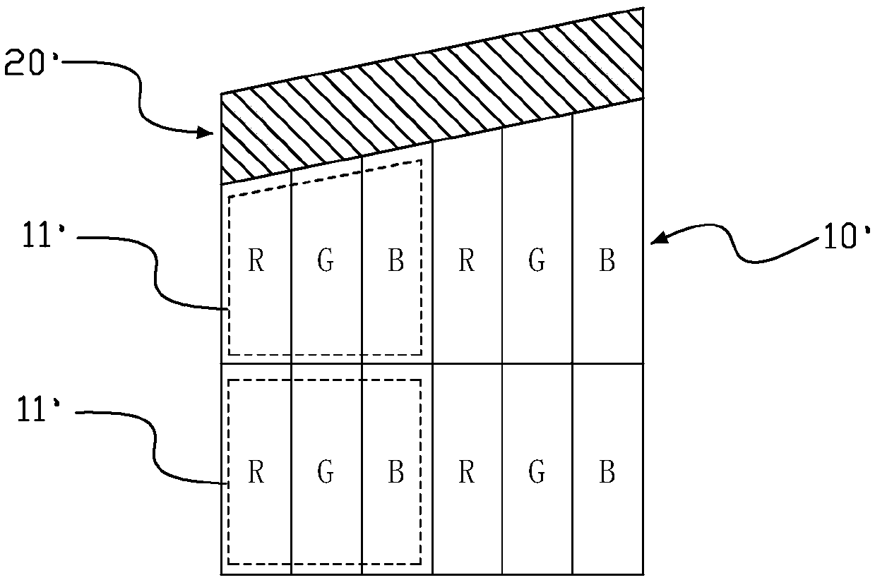
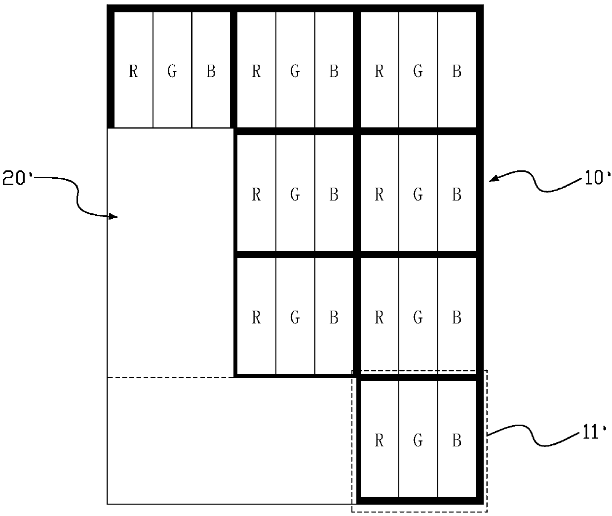
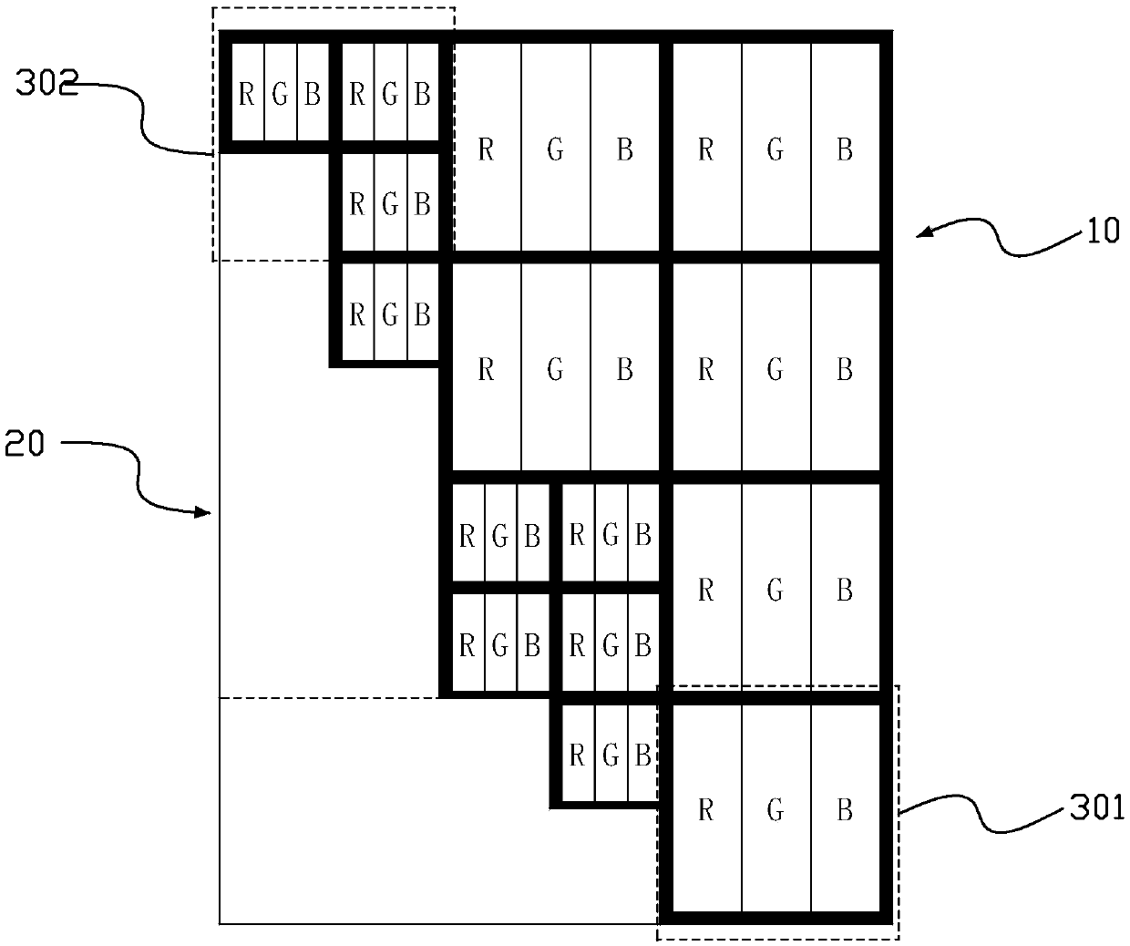
[0033] image 3 is a partial plan view of the liquid crystal display panel in the first embodiment of the present invention, Figure 4 is a schematic diagram of a partial structure on the first substrate in the first embodiment of the present invention, Figure 5 It is a schematic diagram of a partial structure on the second substrate in the first implementation of the present invention. Please refer to Figure 3 to Figure 5 The liquid crystal display panel provided by this embodiment has a display area 10 and a non-display area 20, the non-display area 20 surrounds the display area 10, and the liquid crystal display panel includes a first substrate 30 and a second substrate 40 opposite to the first substrate 30 , the first substrate 30 is provided with a plurality of central pixel units 301 located in the middle of the display area 10 and a plurality of edge pixel units 302 located between the central pixel unit 301 and the non-display area 20, and each central pixel unit 3...

no. 2 example

[0041] Figure 9 is a schematic diagram of a partial structure on the first substrate in the second embodiment of the present invention, Figure 10 for Figure 9 A cross-sectional view along the A-A direction, Figure 11 for Image 6 The cross-sectional view along the B-B direction. Please combine Figure 9 to Figure 11 The difference between this embodiment and the first embodiment is that along the direction toward the second substrate 40, the first substrate 30 is sequentially provided with a common electrode 35, a metal conducting line 31 and an edge pixel electrode 36b, that is, an edge pixel electrode 36b is provided above the common electrode 35 .

[0042] Specifically, combine Figure 10 , along the direction toward the second substrate 40, the first substrate 30 is sequentially provided with a gate insulating layer 306, a data line 34, a first insulating layer 303, a common electrode 35, a second insulating layer 304, and a metal conducting line 31 , the third ...

no. 3 example

[0045] Figure 12 is a schematic diagram of a partial structure on the first substrate in the third embodiment of the present invention, Figure 13 for Figure 12 The cross-sectional view along the direction A-A. Please combine Figure 12 with Figure 13 The difference between this embodiment and the second embodiment is that, along the direction toward the second substrate 40, the first substrate 30 is sequentially provided with metal conduction lines 31, data lines 34, common electrodes 35 and edge pixel electrodes 36b, And each edge pixel electrode 36 b is individually connected to one switching element 37 .

[0046] Specifically, combine Figure 13 , along the direction toward the second substrate 40, the first substrate 30 is sequentially provided with a metal conducting line 31, a gate insulating layer 306, a data line 34, a first insulating layer 303, a common electrode 35, and a second insulating layer 304 and edge pixel electrodes 36b. The scanning lines 33 and...


PUM


Abstract

A liquid crystal display panel comprises a display area and a non-display area, wherein the liquid crystal display panel comprises a first substrate and a second substrate; the first substrate is provided with central pixel units and an edge pixel units; each central pixel unit comprises a plurality of central pixel electrodes; each edge pixel unit comprises a plurality of edge pixel electrodes, the number of the edge pixel electrodes within each edge pixel unit is greater than the number of central pixel electrodes within each central pixel unit; along the direction perpendicular to the firstsubstrate, the regions of the second substrate corresponding to each central pixel unit and each edge pixel unit are provided with a central color-resistance unit and an edge color-resistance unit respectively, and each edge color-resistance unit is filled with a black matrix. According to the invention, a black matrix is utilized to properly cover the area corresponding to each edge pixel electrode on the second substrate, thereby increasing the analytic degree of the edge of the display area so as to reduce the saw tooth phenomenon generated at the edge of the display area.

Description

technical field [0001] The invention relates to the technical field of liquid crystal display, in particular to a liquid crystal display panel. Background technique [0002] With the development of science and technology, people's demand for screen display is more and more diversified. People no longer only meet the conventional performance indicators such as large size and high definition of the display panel, but have higher requirements for the appearance of the display panel. . [0003] At present, the emergence of special-shaped display panels not only makes the display effect more diversified, but also improves the limitation of the single rectangular structure of the display panel. The application of shaped display panels has become more and more widespread, and has been successfully applied to wearable electronic devices such as watches, glasses or smart bracelets. Special-shaped display panels usually have a special-shaped display area, such as a circle, a polygon...

Claims


Application Information

Patent Timeline
Patent Type & Authority Applications(China)
IPC IPC(8): G02F1/1335G02F1/1343G02F1/1362
CPCG02F1/133512G02F1/133514G02F1/134309G02F1/136209G02F1/13624G02F1/136286G02F1/134345
Inventor 房耸蒋隽黄清英
Owner KUSN INFOVISION OPTOELECTRONICS
Why Eureka
Try Eureka