Display screen and array substrate thereof, fingerprint recognition method, and electronic device

An array substrate and fingerprint recognition technology, which is applied in character and pattern recognition, acquisition/organization of fingerprints/palmprints, static indicators, etc., can solve the problem that the sensor cannot collect signals, the volume is shrunk to a small enough size, and the module volume is large, etc. problems, to achieve the effect of improving accuracy, reducing size, and reducing circuit scale

Active Publication Date: 2021-03-16
BOE TECH GRP CO LTD +1
View PDF7 Cites 0 Cited by
  • Summary
  • Abstract
  • Description
  • Claims
  • Application Information

AI Technical Summary

Problems solved by technology

[0002] At present, many mobile phones on the market have added fingerprint recognition function. The fingerprint recognition function can provide functions such as fingerprint unlocking and fingerprint encryption. However, due to the thickness of the screen module, the sensor cannot collect enough useful signals, and the capacitive fingerprint recognition sensor cannot Recognize fingerprints pressed on the screen across the screen
[0003] In related technologies, infrared light fingerprint recognition sensors and ultrasonic fingerprint recognition sensors are used to identify fingerprint lines on the screen, which have strong enough penetration performance, but it means higher power consumption and larger module volume
At present, companies such as OFILM, which provide ultrasonic fingerprint recognition module packaging for Qualcomm, have not been able to reduce the size to a small enough size, and the recognition accuracy and speed also need to be greatly improved.

Method used


Image

  • Display screen and array substrate thereof, fingerprint recognition method, and electronic device
  • Display screen and array substrate thereof, fingerprint recognition method, and electronic device
  • Display screen and array substrate thereof, fingerprint recognition method, and electronic device

Examples


Embodiment Construction

[0044] Embodiments of the present invention are described in detail below, examples of which are shown in the drawings, wherein the same or similar reference numerals designate the same or similar elements or elements having the same or similar functions throughout. The embodiments described below by referring to the figures are exemplary and are intended to explain the present invention and should not be construed as limiting the present invention.

[0045] The display screen and its array substrate, fingerprint identification method, and electronic device according to the embodiments of the present invention will be described below with reference to the accompanying drawings.

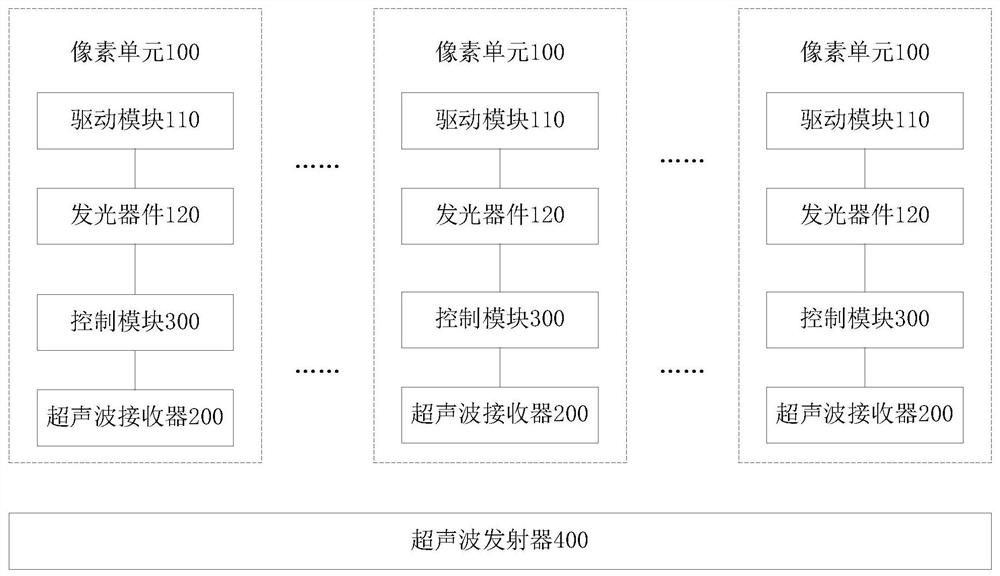
[0046] figure 1 is a schematic block diagram of an array substrate of a display screen according to an embodiment of the present invention. It should be noted that the array substrate of the display screen according to the embodiment of the present invention can be applied in a mobile terminal to rea...


PUM


Abstract

The invention discloses a display screen, an array substrate thereof, a fingerprint identification method, and an electronic device. The array substrate includes: a plurality of pixel units, wherein each pixel unit includes a drive module, a light-emitting device, at least one ultrasonic receiver, and a control panel. Module, the drive module is used to provide driving current to the light-emitting device to drive the light-emitting device to light up; the ultrasonic receiver is used to receive ultrasonic signals; the control module controls the ultrasonic receiver to turn on when the light-emitting device is turned on; the ultrasonic transmitter, the ultrasonic transmitter emits ultrasound. Thus, full-screen fingerprint recognition can be realized, and by integrating the control module of the ultrasonic receiver into the driving circuit of the light-emitting device, the complexity and scale of the circuit can be reduced, and the size of the module can also be reduced. In addition, each Each pixel unit has an ultrasonic receiver, which can greatly improve the accuracy of recognition.

Description

technical field [0001] The invention relates to the technical field of liquid crystal display, in particular to a display screen, an array substrate thereof, a fingerprint identification method, and electronic equipment. Background technique [0002] At present, many mobile phones on the market have added fingerprint recognition function. The fingerprint recognition function can provide functions such as fingerprint unlocking and fingerprint encryption. However, due to the thickness of the screen module, the sensor cannot collect enough useful signals, and the capacitive fingerprint recognition sensor cannot Recognize the fingerprint pressed on the screen across the screen. [0003] In the related art, the infrared fingerprint recognition sensor and the ultrasonic fingerprint recognition sensor are used to recognize the fingerprint pattern on the screen, which has a strong enough penetrating performance, but it means higher power consumption and larger module volume. At pre...

Claims


Application Information

Patent Timeline
Patent Type & Authority Patents(China)
IPC IPC(8): G06K9/00G09G3/20
CPCG09G3/20G06V40/1306
Inventor 禹映雪赵婷婷金美灵李璐璐金正具李良梁郑财辛秦牛亚辉刘雨杰谷林硕
Owner BOE TECH GRP CO LTD
Why Eureka
Try Eureka