A pixel unit and display panel

A technology for pixel units and display panels, applied in electrical components, semiconductor devices, computing, etc., can solve the problems of low light transmittance, small fingerprint recognition area, low recognition accuracy, etc., to save costs, realize full-screen fingerprint recognition, The effect of improving accuracy

Active Publication Date: 2022-07-12
WUHAN CHINA STAR OPTOELECTRONICS SEMICON DISPLAY TECH CO LTD
View PDF11 Cites 0 Cited by
  • Summary
  • Abstract
  • Description
  • Claims
  • Application Information

AI Technical Summary

Problems solved by technology

[0007] The purpose of the present invention is to provide a pixel unit and a display panel, which can solve the problems of long transmission path of reflected light, low light transmittance, low recognition accuracy and small fingerprint recognition area in the existing optical fingerprint recognition.

Method used


Image

  • A pixel unit and display panel
  • A pixel unit and display panel
  • A pixel unit and display panel

Examples


Embodiment 1

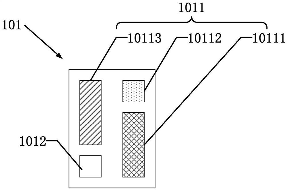
[0048] like figure 2 As shown, this embodiment provides a pixel unit 101 , which includes a light-emitting unit 1011 and a light-sensing unit 1012 .

[0049] like figure 2 As shown, the light-emitting unit includes a red sub-pixel 10111 , a green sub-pixel 10112 and a blue sub-pixel 10113 .

[0050] like figure 2As shown, the distance between the photosensitive unit 1012 and the green sub-pixel 10112 is greater than the distance between the photosensitive unit 1012 and the red sub-pixel 10111; and is greater than the distance between the photosensitive unit 1012 and the blue sub-pixel 10113 . That is, the photosensitive unit 1012 in the pixel unit 101 is the farthest from the green sub-pixel 10112 . Since in the prior art, the material of the photosensitive layer at the photosensitive unit 1012 is more sensitive to green light than to red and blue light, the photosensitive unit 1012 is arranged at the farthest position from the green sub-pixel 10112, The interference o...

Embodiment 2

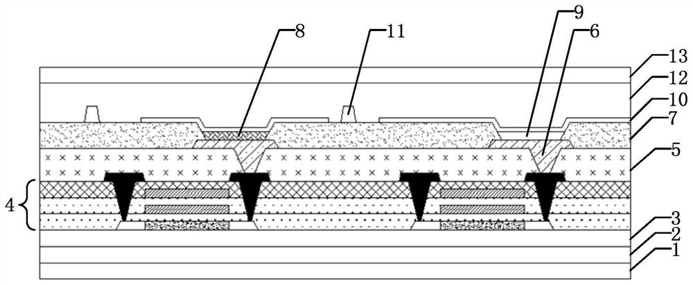
[0075] like Image 6 As shown, this embodiment includes most of the technical features of Embodiment 1. The difference between this embodiment and Embodiment 1 is that the display panel 100 provided by this embodiment further includes a second pixel unit 102 .

[0076] like Image 6 As shown, the second pixel unit 102 only includes the light-emitting unit 1011, that is, the second pixel unit is not provided with a photosensitive unit 1012.

[0077] like Image 6 As shown, the pixel unit 101 and the second pixel unit 102 are arranged in a matrix. Therefore, the pixel units 101 with the photosensitive units 1012 are evenly distributed throughout the display panel 100, and the pixel units 101 and the second pixel units 102 are arranged at intervals, so that the entire display panel 100 is a fingerprint recognition area, so as to realize full-screen fingerprint recognition and increase the The fingerprint recognition area is increased, and the customer experience is improved. ...


PUM


Abstract

The invention relates to a pixel unit and a display panel. First, a photosensitive layer is prepared on a pixel electrode layer by using an organic material, which is used to receive the reflected light generated by the light-emitting layer irradiating the fingerprint ridges and valleys, and shorten the light-emitting layer irradiating the fingerprint ridge. The transmission path of the reflected light generated by the ridges and valleys improves the accuracy of fingerprint identification; secondly, the photosensitive layer in the present invention generates induced currents of different sizes after receiving the reflected light generated by the light-emitting layer irradiated on the ridges and valleys of the fingerprint. The induced current is transmitted to the source and drain layers through the pixel electrode layer, and then to the external processing system through the active layer, etc. Therefore, the present invention does not need to add an additional fingerprint identification module, which greatly saves the cost; in addition, in the present invention The pixel units with photosensitive units are evenly distributed on the entire display panel, so that the entire display panel is a fingerprint recognition area, so as to realize full-screen fingerprint recognition.

Description

technical field [0001] The present invention relates to the field of display technology, in particular to a pixel unit and a display panel. Background technique [0002] The display device can convert the data of the computer into various characters, numbers, symbols or intuitive images for display, and can use input tools such as keyboards to input commands or data into the computer, and add, delete, and change the display at any time with the help of the hardware and software of the system. content. Display devices are classified into plasma, liquid crystal, light emitting diode, and cathode ray tube types according to the display device used. [0003] Organic light-emitting display devices (English full name: Organic Light-Emitting Diode, OLED for short) are also known as organic electric laser display devices and organic light-emitting semiconductors. The working principle of OLED is: when the power is supplied to an appropriate voltage, the positive hole and the negat...

Claims


Application Information

Patent Timeline
Patent Type & Authority Patents(China)
IPC IPC(8): H01L27/32G06V40/13
CPCG06V40/12H10K59/35H10K59/60H10K59/121
Inventor 应俊
Owner WUHAN CHINA STAR OPTOELECTRONICS SEMICON DISPLAY TECH CO LTD
Why Eureka
Try Eureka