Circuit Board Assembly Having Passive Component and Stack Structure Thereof

a technology of circuit board and component, which is applied in the association of printed electric components, printed circuit non-printed electric components, semiconductor/solid-state device details, etc., can solve the problems of limiting the enhancement and development of the electricity function of the carrier board, short circuits, etc., and achieves the enhancement of the electric function and the transmission efficiency between electronic components, the effect of reducing the module size and efficient utilization of the carrier board spa

Inactive Publication Date: 2008-02-28
PHOENIX PRECISION TECH CORP
View PDF23 Cites 16 Cited by
  • Summary
  • Abstract
  • Description
  • Claims
  • Application Information

AI Technical Summary

Benefits of technology

[0016]In the present invention, the carrier board is embedded with a semiconductor component and integrated with a passive component. Accordingly, the electricity function and the transmission efficiency between electron

Problems solved by technology

That is, die bonding process and wire bonding process for each layer semiconductor chip must be separately performed, which is accordingly rather complicated.
Meanwhile, as evenness of the adhesive layer 24 is difficult to control, it may occur that the second semiconductor chip 22b contact

Method used


Image

  • Circuit Board Assembly Having Passive Component and Stack Structure Thereof
  • Circuit Board Assembly Having Passive Component and Stack Structure Thereof
  • Circuit Board Assembly Having Passive Component and Stack Structure Thereof

Examples


first embodiment

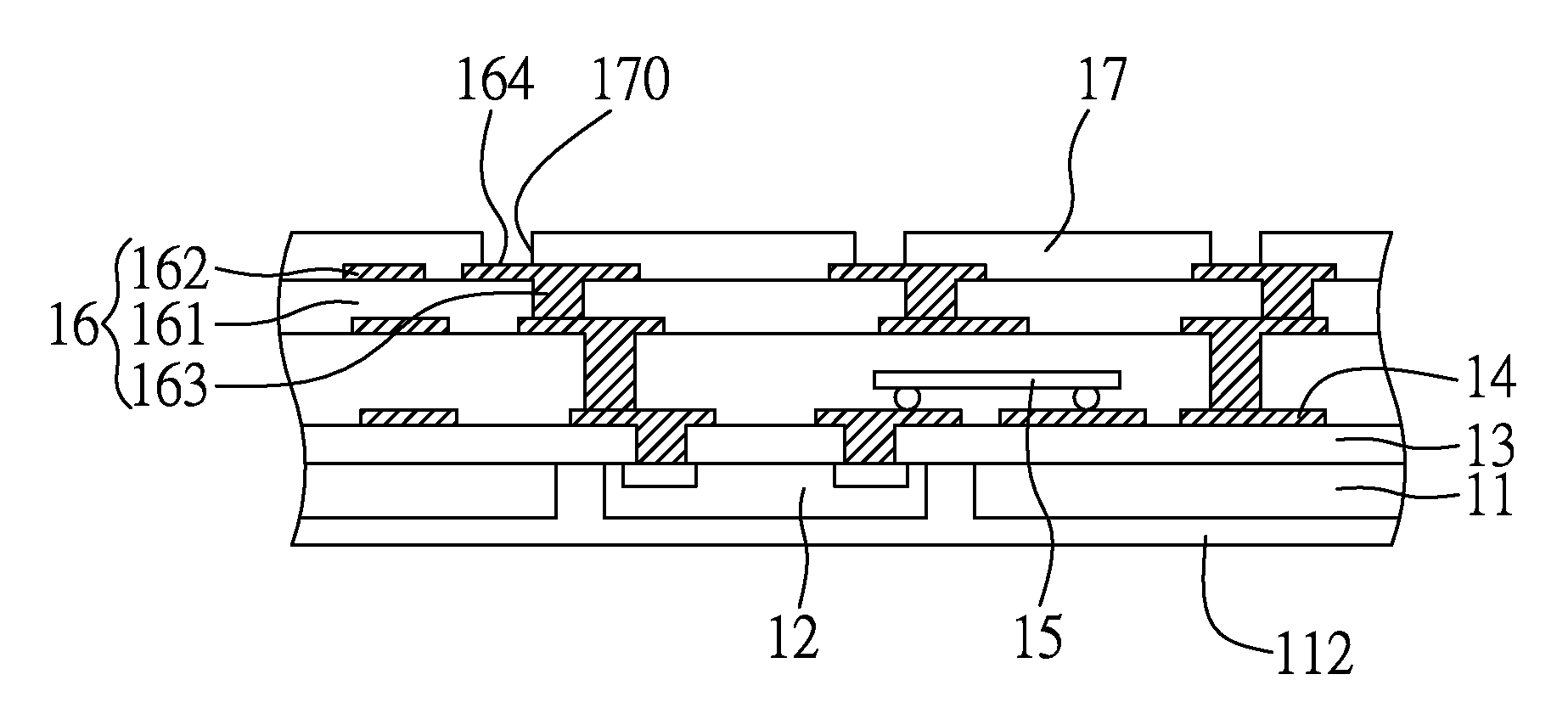
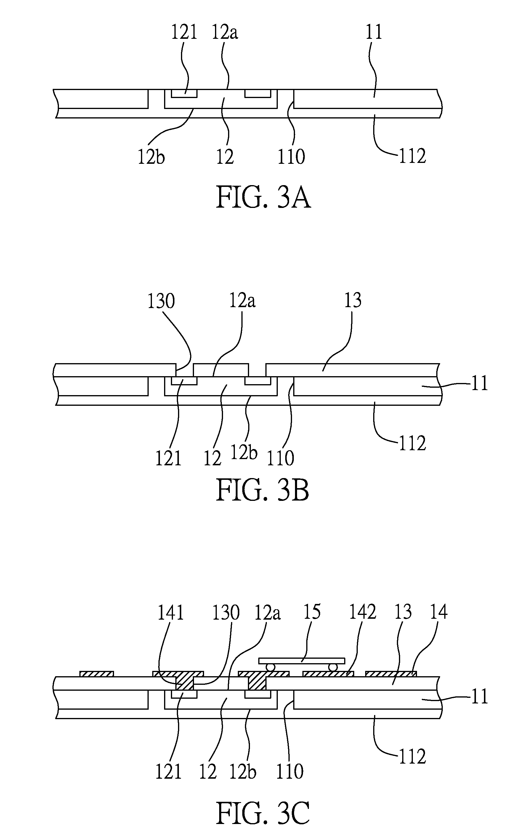
[0022]FIGS. 3A to 3D show a fabrication process of a circuit board structure having a passive component according to a first embodiment of the present invention.

[0023]As shown in FIG. 3A, a carrier board 11 formed with at least one through opening 110 is provided. The carrier board 11 may be a metal board, a dielectric board, or a circuit board having circuits thereon. A semiconductor component 12 having an active surface 12a is received in the through opening 110, wherein the active surface 12a of the semiconductor component 12 has a plurality of electrode pads 121 formed thereon. The semiconductor component 12 can be an active component such as a CPU, a DRAM, a SRAM or a SDRAM. An adhesive layer 112 is formed on one surface of the carrier board 11 that is opposite to the active surface 12a of the semiconductor component 12, and the adhesive layer 112 is used to fill in gaps between the opening 110 and the semiconductor component 12 for securing in position the semiconductor compon...

second embodiment

[0030]FIG. 4 shows a stack structure of a circuit board assembly having at least a passive component according to a second embodiment of the present invention. As shown in FIG. 4, the stack structure of the circuit board assembly comprises: at least two carrier boards 11, 11′ each having a through opening 110,110′ respectively for receiving semiconductor components 12, 12′ in the openings 110,110′, the semiconductor components 12, 12′ respectively having active surfaces 12a, 12a′ and non-active surfaces 12b, 12b′ and the active surfaces 12a, 12a′ respectively have a plurality of electrode pads 121,121′, the two carrier boards 11, 11′ as the non-active surfaces 12b, 12b′ of the semiconductor components 12, 12′ and the non-active surfaces 12b, 12b′ of the semiconductor components 12, 12′ are combined together by an adhesive layer 18; dielectric layers 13, 13′ respectively formed on the active surfaces 12a, 12a′ of the semiconductor components 12, 12′ as well as surfaces of the carrier...


PUM


Abstract

A circuit board assembly having at least a passive component and a stack structure of the circuit board are disclosed, including: a carrier board formed with a through opening for receiving a semiconductor component having an active surface on which electrode pads are formed; a dielectric layer formed on the carrier board and the semiconductor component and formed with openings to expose the electrode pads; a circuit layer formed on the dielectric layer and having conductive structures formed in the openings of the dielectric layer for electrically connecting the electrode pads, and a plurality of lands for mounting at least one passive component electrically connected to the circuit layer; and a circuit build-up structure formed on the dielectric layer, the circuit layer and the passive component, with conductive structures formed for electrically connecting the circuit layer.

Description

BACKGROUND OF THE INVENTION[0001]1. Field of the Invention[0002]The present invention relates generally to a circuit board structure having passive component and stack structure thereof, and more particularly to a circuit board structure integrated with semiconductor component and passive component, and stack structure thereof.[0003]2. Description of Related Art[0004]For consequent reduction in size of electronic components, much more semiconductor components having different functions are required to be embedded in a circuit board. To meet the requirement, a chip carrier of a semiconductor package such as a substrate or a leadframe must be mounted and electrically connected with at least two semiconductor chips, wherein the semiconductor chips are stack mounted on the chip carrier and electrically connected to the chip carrier by solder wires.[0005]FIG. 1 is a sectional diagram of a multi-chip semiconductor package 2 disclosed by U.S. Pat. No. 5,323,060. As shown in FIG. 1, a first...

Claims


Application Information

Patent Timeline
IPC IPC(8): H05K1/09H05K1/16H05K1/18
CPCH01L23/50H01L2224/48227H01L24/24H01L24/82H01L2224/24227H01L2224/48091H01L2924/01013H01L2924/01015H01L2924/01056H01L2924/01082H01L2924/04953H01L2924/19041H01L2924/19042H01L2924/19043H05K1/023H05K1/185H05K3/4602H05K2201/09536H05K2201/10674H01L23/5389H01L24/19H01L24/48H01L2924/01006H01L2924/01024H01L2924/01033H01L2924/01047H01L2924/014H01L2924/00014H01L2224/04105H01L2224/32145H01L2224/73265H01L2924/15153H01L2924/00H01L2224/45099H01L2224/45015H01L2924/207
Inventor LIEN, CHUNG-CHENGCHANG, CHIA-WEI
Owner PHOENIX PRECISION TECH CORP
Why Eureka
Try Eureka