A kind of array substrate and display panel

A technology for array substrates and display areas, applied to static indicators, identification devices, instruments, etc., can solve the problems of limited size and large coupling capacitance

Active Publication Date: 2020-07-07
XIAMEN TIANMA MICRO ELECTRONICS
View PDF6 Cites 0 Cited by
  • Summary
  • Abstract
  • Description
  • Claims
  • Application Information

AI Technical Summary

Problems solved by technology

[0003] Usually, the data lines corresponding to the sub-pixels located under the opening need to bypass the opening, and the size of the wiring area surrounding the opening on the full screen is limited, so that the line spacing between the data lines located in the wiring area is smaller than that of the display. The line spacing of adjacent data lines in the area, which leads to a large coupling capacitance between adjacent data lines in the wiring area

Method used


Image

  • A kind of array substrate and display panel
  • A kind of array substrate and display panel
  • A kind of array substrate and display panel

Examples


Embodiment Construction

[0033] The following will clearly and completely describe the technical solutions in the embodiments of the present invention with reference to the accompanying drawings in the embodiments of the present invention. Obviously, the described embodiments are only some, not all, embodiments of the present invention. Based on the embodiments of the present invention, all other embodiments obtained by persons of ordinary skill in the art without making creative efforts belong to the protection scope of the present invention.

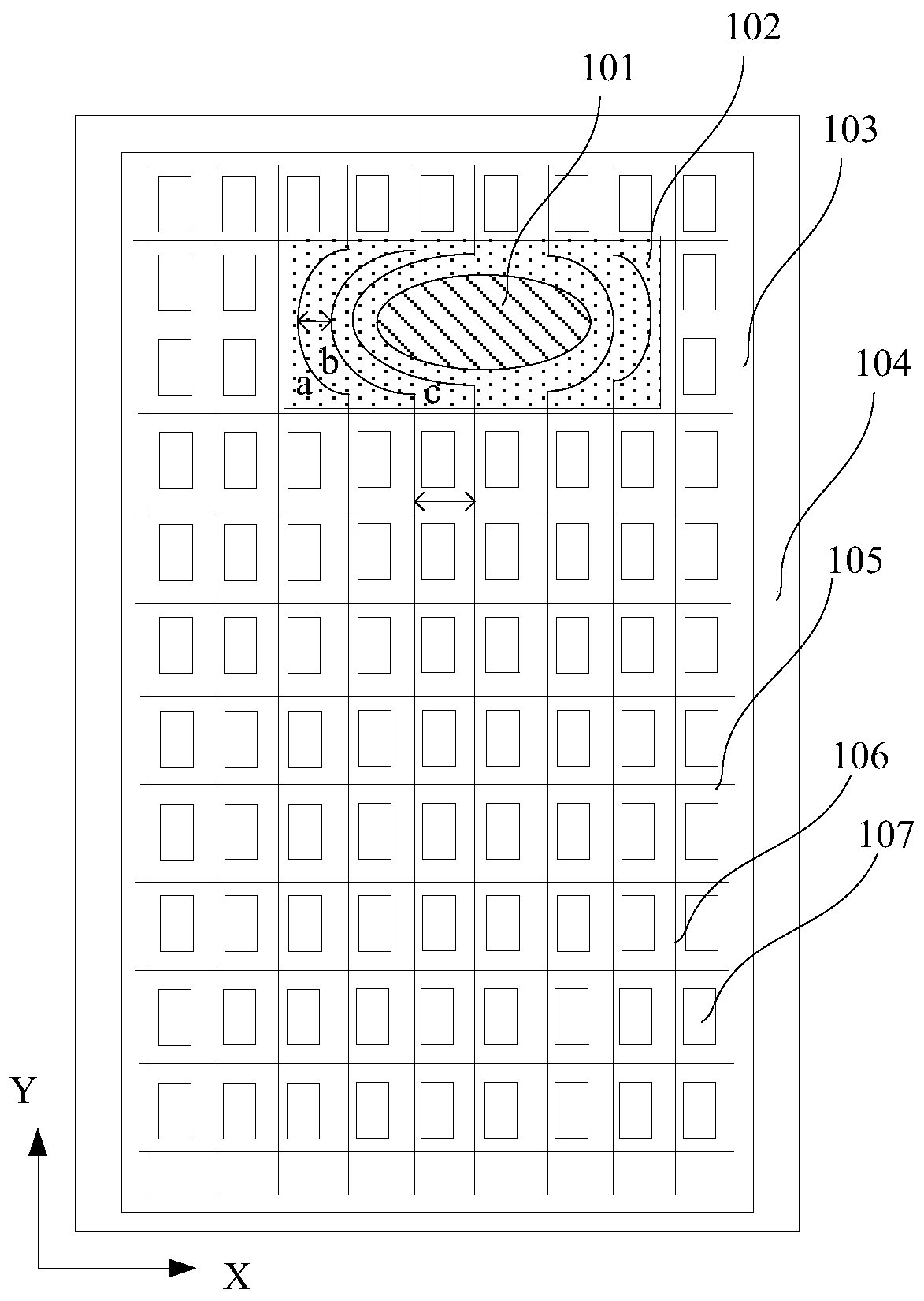
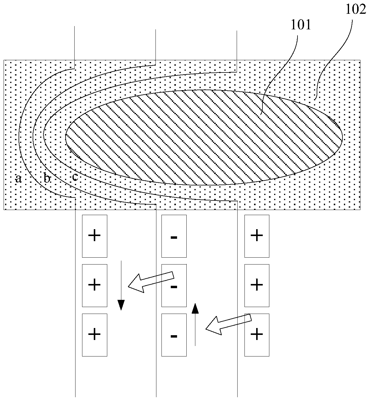
[0034] see figure 1 , figure 1 It is a structural schematic diagram of a full screen in the prior art. The full screen includes an aperture area 101 , a wiring area 102 surrounding the opening area 101 , a display area 103 surrounding the wiring area 102 , and a non-display area 104 surrounding the display area 103 . In addition, the full screen also includes a plurality of gate lines 105 and a plurality of data lines 106 arranged in the display area 103, wh...


PUM


Abstract

The present invention provides an array substrate and a display panel. The array substrate includes a non-display area and a display area. The non-display area includes a first non-display area and a second non-display area. The display area includes a normal display area and a wiring area; A non-display area surrounds the normal display area, the normal display area surrounds the wiring area, the wiring area surrounds the second non-display area, and the second non-display area includes the opening area. In this solution, the data wires corresponding to the sub-pixels that are charged at the same time are overlapped, so that the number of data wires located in the same layer of the wiring area is reduced, the area of ​​the wiring area is reduced, and the second non-display area and the normal display area are realized. Narrow bezel design between. Moreover, since the number of data leads in the same layer in the wiring area is reduced, the line spacing between adjacent data leads is increased, thereby reducing the coupling capacitance between adjacent data leads in the same layer.

Description

technical field [0001] The present invention relates to the field of display technology, and more specifically, to an array substrate and a display panel. Background technique [0002] With the rapid development of narrow bezels of display screens, full screens have emerged as the times require. Since the display screen usually has components such as a front camera, a speaker, an indicator light, and a sensor, holes need to be opened in the display area of ​​the full screen. [0003] Usually, the data lines corresponding to the sub-pixels located under the opening need to bypass the opening, and the size of the wiring area surrounding the opening on the full screen is limited, so that the line spacing between the data lines located in the wiring area is smaller than that of the display. The line spacing between adjacent data lines in the wiring area leads to a large coupling capacitance between adjacent data lines in the wiring area. [0004] Therefore, how to provide an a...

Claims


Application Information

Patent Timeline
Patent Type & Authority Patents(China)
IPC IPC(8): H01L27/12H01L27/32G09F9/00
CPCG09F9/00H01L27/12H01L27/124H10K59/353H10K59/1216H10K59/131G09G3/3614G09G2300/0426G09G2310/0297G09G3/20G09G2300/0452G09G2320/0209G09G2310/0254H10K59/40G09G2310/0251G09G2310/08
Inventor 贝亮亮伍黄尧蓝学新周洪波朱绎桦赖国昌陈国照
Owner XIAMEN TIANMA MICRO ELECTRONICS
Why Eureka
Try Eureka