
Fingerprint identification device and manufacturing method thereof

A technology for fingerprint identification and manufacturing method, which is applied in the acquisition/organization of fingerprints/palmprints, character and pattern recognition, and the use of vibrating fluids, etc., and can solve problems such as increased noise

Inactive Publication Date: 2018-11-16
RECO TECH CHENGDU CO LTD
View PDF5 Cites 2 Cited by
  • Summary
  • Abstract
  • Description
  • Claims
  • Application Information

AI Technical Summary

Problems solved by technology

When performing fingerprint recognition, this concave-convex microstructure causes a small gap between the finger and the conductive layer, resulting in an increase in noise

Method used


Image

  • Fingerprint identification device and manufacturing method thereof
  • Fingerprint identification device and manufacturing method thereof
  • Fingerprint identification device and manufacturing method thereof

Examples


Embodiment Construction

[0034] In order to make the description of the present disclosure more detailed and complete, the following provides an illustrative description of the implementation aspects and specific embodiments of the present invention; but this is not the only form of implementing or using the specific embodiments of the present invention. The various embodiments disclosed below can be combined or replaced with each other when beneficial, and other embodiments can also be added to one embodiment, without further description or illustration. In the following description, numerous specific details will be set forth in order to enable readers to fully understand the following embodiments. However, embodiments of the invention may be practiced without these specific details.

[0035] The embodiments of the present invention are described in detail below, but the present invention is not limited to the scope of the examples.

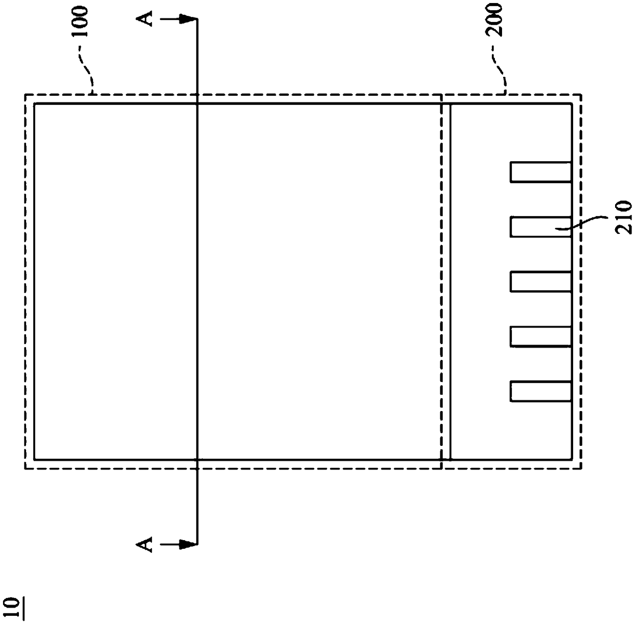
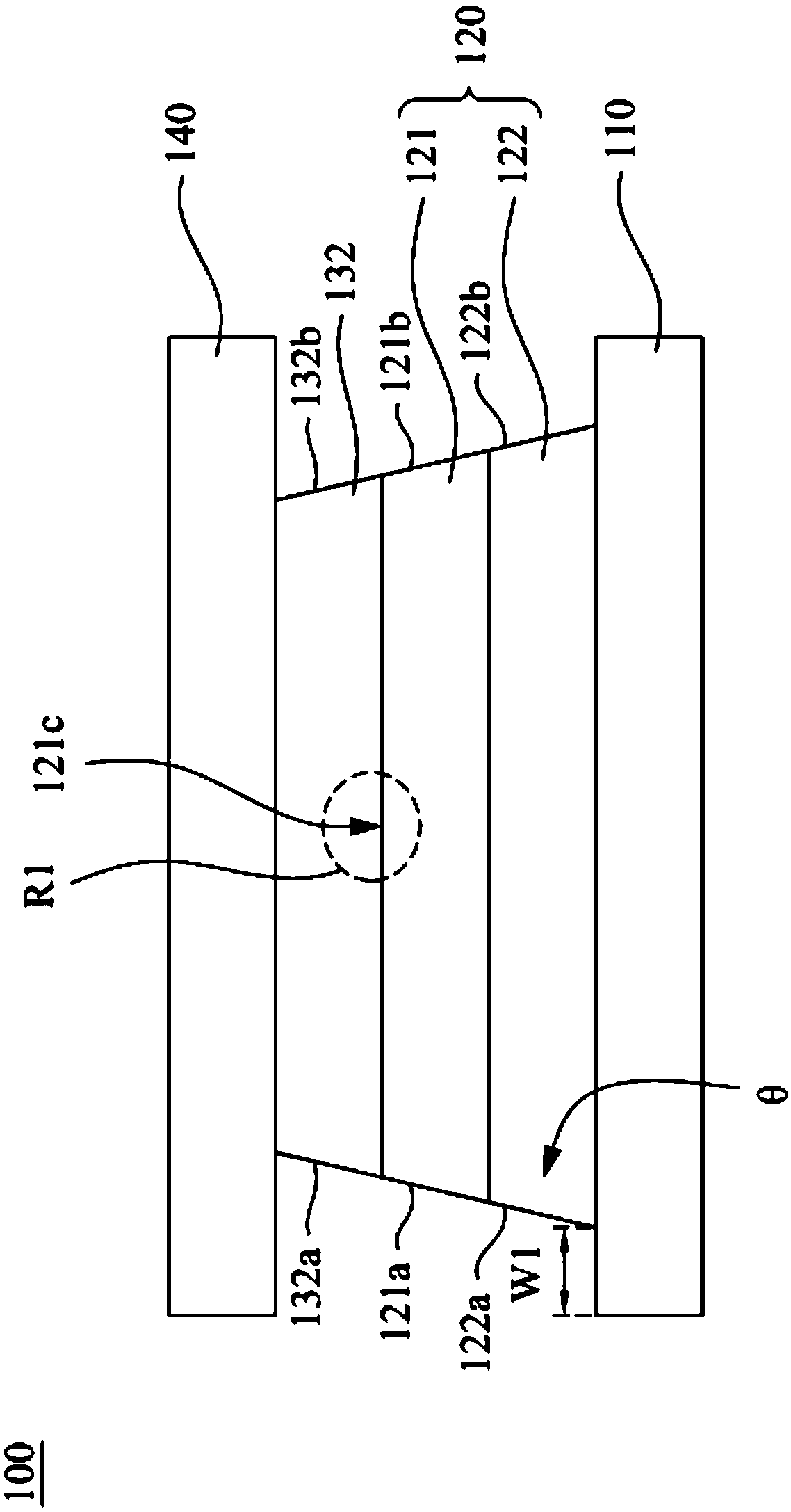
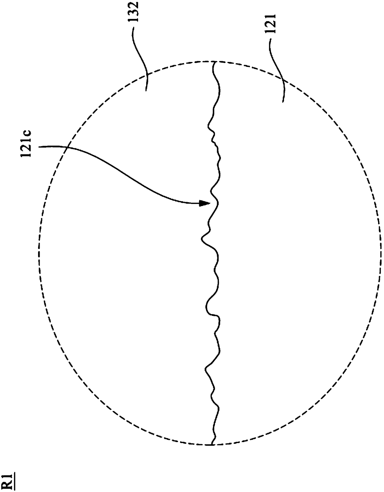
[0036] figure 1 A schematic top view of the fingerprint identif...


PUM


Abstract

The invention relates to a fingerprint identification device which comprises a substrate, a piezoelectric layer, a conducting layer and a flat layer. The piezoelectric layer is arranged on the substrate. The conducting layer is arranged on the piezoelectric layer, and the conducting layer is provided with a concave-convex micro structure and the concave-convex micro structure is positioned on an upper surface of the conducting layer. The flat layer is arranged on the conducting layer, and one bottom of the flat layer fills up the concave-convex micro structure of the conducting layer. The flatlayer can reduce noise, and scratches and oxidation of the conducting layer are avoided.

Description

technical field [0001] The present invention relates to a fingerprint identification device and a method for manufacturing the fingerprint identification device. Background technique [0002] Fingerprint identification devices have been widely used in different fields such as industry, national defense, fire protection, and electronics. However, limited by the material properties and manufacturing process of the conductive layer in the fingerprint identification device, the formed conductive layer has a concave-convex microstructure on the surface of the conductive layer. When fingerprint recognition is performed, the concave-convex microstructure causes a small gap between the finger and the conductive layer, resulting in increased noise. Contents of the invention [0003] An aspect of the present invention provides a fingerprint recognition device, which includes a substrate, a piezoelectric layer, a conductive layer, and a flat layer. The piezoelectric layer is dispos...

Claims


Application Information

Patent Timeline
Patent Type & Authority Applications(China)
IPC IPC(8): G06K9/00G06V10/147H10N30/00H10N30/088H10N30/857
CPCG06V40/1306B06B1/0622B06B1/0677G06V10/147H10N30/088H10N30/857H10N30/101
Inventor 谢佩君卢宏杰
Owner RECO TECH CHENGDU CO LTD
Features
  • Generate Ideas
  • Intellectual Property
  • Life Sciences
  • Materials
  • Tech Scout
  • Unparalleled Data Quality
  • Higher Quality Content
  • 60% Fewer Hallucinations
Learn More