A method for detecting and classifying pixel defects in inkjet printing of a printed display panel and a device thereof

A printing display and inkjet printing technology, used in image analysis, image enhancement, image data processing, etc., can solve the problems of inaccurate positioning, poor consistency, low efficiency, etc., to improve product quality and yield, and reduce subsequent processing. cost effect

Inactive Publication Date: 2018-12-11
FUZHOU UNIV
View PDF8 Cites 27 Cited by
  • Summary
  • Abstract
  • Description
  • Claims
  • Application Information

AI Technical Summary

Problems solved by technology

[0004] The object of the present invention is to provide a method and device for detecting and classifying pixel defects in inkjet printing of a printed display panel, aiming to solve problems such as manual detection and classification of nozzle ejection direction deviation, satellite ink droplet, inaccurate positioning, large ink droplet size, etc. The problems of typical defects such as poor film uniformity are long time, low efficiency, test results are easily affected by human subjective factors, and poor consistency

Method used


Image

  • A method for detecting and classifying pixel defects in inkjet printing of a printed display panel and a device thereof
  • A method for detecting and classifying pixel defects in inkjet printing of a printed display panel and a device thereof

Examples


Embodiment Construction

[0031] The technical solution of the present invention will be specifically described below in conjunction with the accompanying drawings.

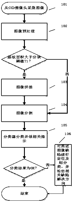
[0032] The present invention provides a method for detecting and classifying pixel defects in inkjet printing of a printed display panel, comprising the following steps:

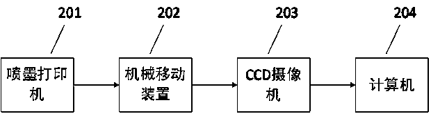
[0033] Step S1, placing the printed display panel after inkjet printing on the detection platform, and obtaining the original image of the printed display panel to be detected in blocks;

[0034] Step S2, preprocessing the block original image received in step S1;

[0035] Step S3, stitching all the block original images of the same printed display panel after preprocessing;

[0036] Step S4, segmenting the spliced ​​original image to obtain a detection target;

[0037] Step S5, for the segmented original image, use the SVM classifier in machine learning to perform binary classification on the image, if there is no defective pixel, then perform the follow-up process, ...


PUM


Abstract

The invention relates to a method for detecting and classifying pixel defects in inkjet printing of a printed display panel and a device thereof. The method comprises the following steps: obtaining the image of a panel to be tested in blocks; when an original image is received, preprocessing the original image; when the pre-processed original image is received, stitching all the partitioned imagesof the same panel ; when the original image is received, segmenting the image is segmented; when the segmented original image is received, using a classifier in machine learning to classify the image, if there is no defect, the image entering the subsequent process, and if there is any, giving the prompt; when the original image of the defective pixel is prompted after the classification is received, positioning and subclassifying the defective pixel of the image, and carrying out statistical analysis of the category and the number of the defective pixels of the image to indicate corresponding defects. The invention aims at solving the problems that the manual detection and classification exist for a long time, the efficiency is low, the detection result is easy to be influenced by humansubjective factors, and the consistency is poor.

Description

technical field [0001] The invention relates to a detection device for a printed display panel, in particular to a method for detecting and classifying pixel defects in inkjet printing of a printed display panel and a device thereof. Background technique [0002] Printed display panels such as Organic-Emitting Diode (OLED) displays, Quantum Dot Light Emitting Diodes (QLED) displays, and printed Electrowetting Displays (Electrowetting Display, EWD) displays are widely used due to their active light emission and low power consumption. , wide viewing angle, low cost, and easy realization of flexible display have attracted more and more attention from the display industry, representing the development direction of future display technology. However, due to the cumbersome and complicated process of printing display panels, various defects inevitably appear in the product, which limits the printing accuracy and process stability, and ultimately leads to an extremely low product yi...

Claims


Application Information

Patent Timeline
Patent Type & Authority Applications(China)
IPC IPC(8): G06T7/00G06T7/10G06T3/40
CPCG06T3/4038G06T7/0004G06T7/10G06T2207/20084G06T2207/20081G06T2207/30141
Inventor 林志贤纪艳玲唐谦林珊玲郭太良
Owner FUZHOU UNIV
Why Eureka
Try Eureka