Supercharge Your Innovation With Domain-Expert AI Agents!

Packaging mold and semiconductor packaging process

A semiconductor and mold technology, applied in the field of semiconductor packaging process, can solve the problem that the mold flow of the colloid cannot completely cover the upper and lower surfaces of the substrate

Active Publication Date: 2022-07-08
ADVANCED SEMICON ENG INC
View PDF18 Cites 0 Cited by
  • Summary
  • Abstract
  • Description
  • Claims
  • Application Information

AI Technical Summary

Problems solved by technology

[0007] This disclosure relates to a packaging mold and a semiconductor packaging process, which can solve the problem that the mold flow of the colloid cannot completely cover the upper and lower surfaces of the substrate caused by the use of conventional molds

Method used


Image

  • Packaging mold and semiconductor packaging process
  • Packaging mold and semiconductor packaging process
  • Packaging mold and semiconductor packaging process

Examples


Embodiment Construction

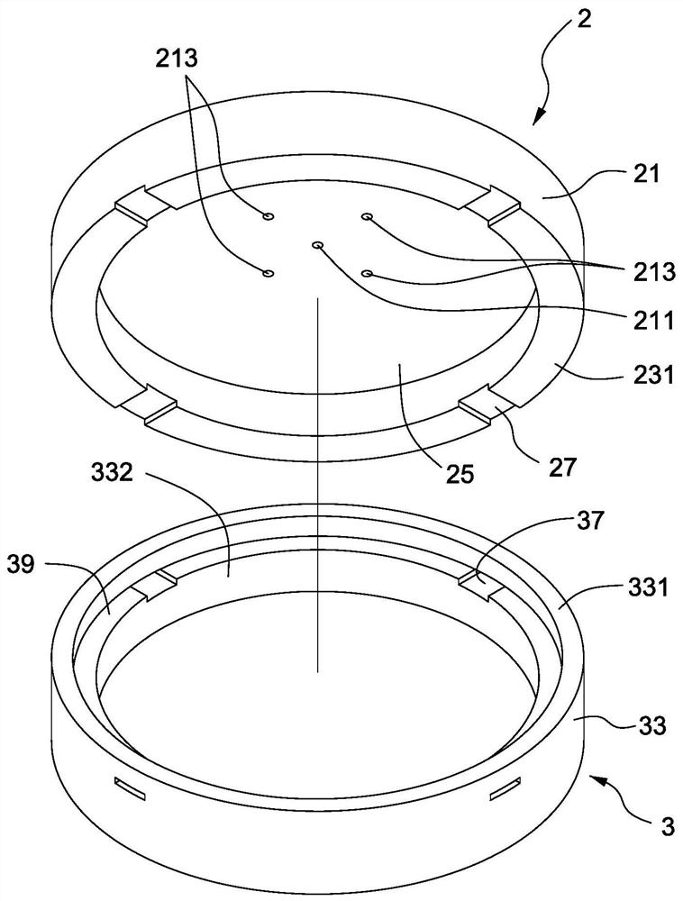
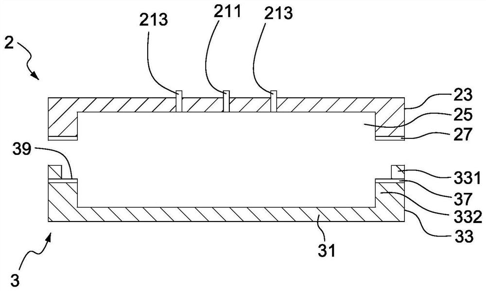
[0015] figure 1 A schematic exploded perspective view of an embodiment of the packaging mold of the present disclosure, and figure 2 It is a schematic exploded cross-sectional view of an embodiment of the packaging mold of the present disclosure. see figure 1 and figure 2 , the packaging mold 1 has an upper mold 2 and a lower mold 3 that can be separated and combined with each other, the user can separate the upper mold 2 and the lower mold 3, and place the object to be packaged in them, and then put the upper mold 2 Combined with the lower mold 3 to carry out the packaging process of the object.

[0016] like figure 1 and figure 2 As shown, the upper mold 2 has an upper part 21 and an upper side part 23 combined with the upper part 21 , and a space that the upper part 21 and the upper side part 23 of the upper mold 2 can jointly define is an upper mold cavity 25 . The upper part 21 of the upper mold cavity 2 has a main glue injection port 211 and a plurality of secon...


PUM


Abstract

The present disclosure relates to a packaging mold for semiconductor packaging, which includes a first mold and a second mold. The first mold has an upper portion, at least one injection port disposed on the upper portion, an upper side portion connected to the upper portion, a first mold cavity formed between the upper portion and the upper side portion, and a cavity formed in the upper portion. The upper side part penetrates at least one first exhaust hole of the upper side part. The second mold has a lower portion, a lower side portion connected to the lower portion, a second cavity formed between the lower portion and the lower side portion, at least one cavity formed on the lower side portion and penetrating the lower side portion The second vent hole and a support portion located in the second mold cavity and formed on the lower side portion, wherein the support portion is used to support an object to be packaged.

Description

technical field [0001] The present disclosure relates to a packaging mold, especially for a semiconductor packaging process. Background technique [0002] In the current field of semiconductor packaging process technology, the multi-side molding technology can effectively improve the utilization rate of the substrate and reduce the area of ​​the substrate. Multi-side molding technology can become the development trend of the semiconductor industry. [0003] Regarding the mold design currently used in the multi-side molding technology, there are injection ports on the side of the mold, and vent holes are provided at appropriate places in the mold, and the mold is placed in the mold. The substrate to be encapsulated is provided with a through hole at an appropriate position. In this way, the substrate placed in the mold can be encapsulated by means of transfer molding. [0004] If the through hole set on the substrate is closer to the injection port of the mold, and the vent...

Claims


Application Information

Patent Timeline
Patent Type & Authority Patents(China)
IPC IPC(8): H01L21/56B29C45/27B29C45/32B29C45/34
CPCH01L21/565B29C45/2701B29C45/32B29C45/34
Inventor 赖晋圆陈瑭原杨金凤陈柏勋
Owner ADVANCED SEMICON ENG INC
Features
  • R&D
  • Intellectual Property
  • Life Sciences
  • Materials
  • Tech Scout
  • Unparalleled Data Quality
  • Higher Quality Content
  • 60% Fewer Hallucinations
Learn More