Semicondutor laser device and its manufacturing method

a semiconductor and laser technology, applied in the direction of lasers, semiconductor laser structural details, semiconductor lasers, etc., can solve the problems of laser beam blocking, poor laser beam output, and hardly formed reflective films

Inactive Publication Date: 2004-11-25
NICHIA CORP
View PDF1 Cites 207 Cited by
  • Summary
  • Abstract
  • Description
  • Claims
  • Application Information

AI Technical Summary

Problems solved by technology

In the case of such substrates, it is difficult to form the resonator faces by cleaving the semiconductor layer with the help of the cleavability of the substrates, and therefore, the resonator faces are often formed by etching.
For obtaining chips thereafter, the substrates are split by applying physical force through a means of scribing and the like because it is difficult to etch sapphire of the substrates.
However, where the resonator faces are formed by etching, there is a problem in that satisfactory reflective films are hardly formed because the end faces are uneven.
For this reason, there is a problem in that, even if the resonator faces of the semiconductor layer have an excellent mirror surface, the output can be poor according to the quality of the reflective films formed on the resonator faces.
There is also a problem in that a laser beam is blocked because of the uneven end faces and the far field pattern (FFP) is disturbed.
With this construction, part of the beam may interfere at the projection.
Such a projection is hard to form if the resonator face is formed by cleavage.
However, if the distance is too small, severe conditions on alignment accuracy and the like need to be satisfied at photolithography.
Also it is difficult to form the protective film and the like, and the resonator face is liable to be roughened at etching.
As a result, mass-productivity is not high.
In other words, if the projection is projected from a position at a distance sufficiently far from the active layer, the above problem becomes insignificant.
Thus, the light from the resonator face becomes unliable to be cut off.
Particularly, it is difficult to divide a gallium nitride semiconductor layer that is grown on a hetero substrate and is difficult to cleave, at a targeted position, and it is difficult to control the distance from the resonator face to the end face of the projection.
If the projection is to be formed closely to the resonator face, the formation thereof needs to be done accurately, costs increase correspondingly and the yield worsens.
Where the protective film is not continuous, light potentially reflected inside may be emitted therefrom, which adversely affect the FFP.
These lights, if mixed with the laser beam, disturb the FFP.
Therefore, light propagating through the inside of the protective film is released in the same direction as the laser beam and is mixed with the laser beam, which deteriorates the FFP.
However, on the monitor side, the protective film may not be formed on the end face of the projection.
If such light is mixed with the main beam, the FFP worsens.
Although the light amplified by the exposed end face of the projection of the semiconductor layer is weak, it will be obtrusive when it is mixed with weak light at the foot of the spectrum of the main beam.
Particularly, where the projection on the emission side is exposed, impurities in the air (for example, carbon, etc.) may adhere to the end face of the projection, deteriorate the end face and adversely affect the semiconductor layer.
In some cases, the impurities cause heat, which propagates to the resonator face and raises the temperature of the resonator face.
That can be a cause of deterioration.
In the first end-face etch step, if etch depth is large, the resonator face previously formed are roughened and a mirror face is hard to obtain.
If the protective film is formed before coverage with the mask, that causes the problem that the protective film is not formed on the end face of the projection.
Also there is a problem in that the material of the mask is roughened by the second end-face etch step and even the protective film is roughened.

Method used


Image

  • Semicondutor laser device and its manufacturing method
  • Semicondutor laser device and its manufacturing method
  • Semicondutor laser device and its manufacturing method

Examples


example 1

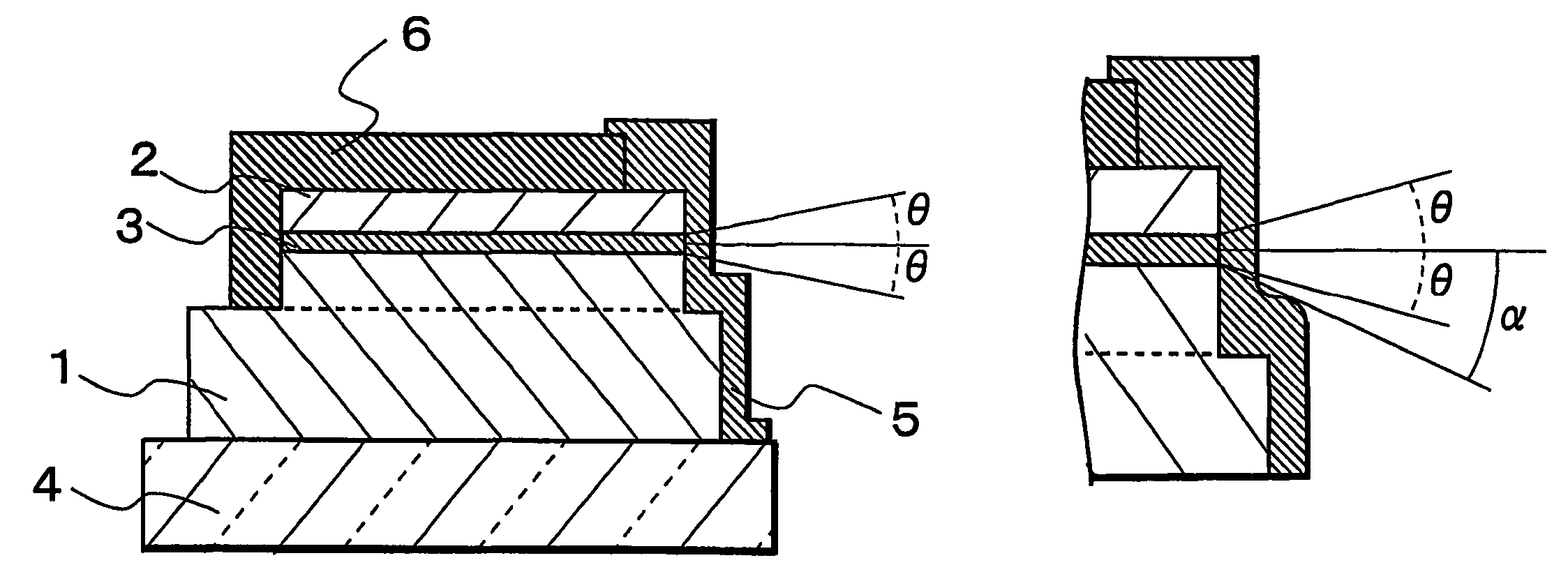
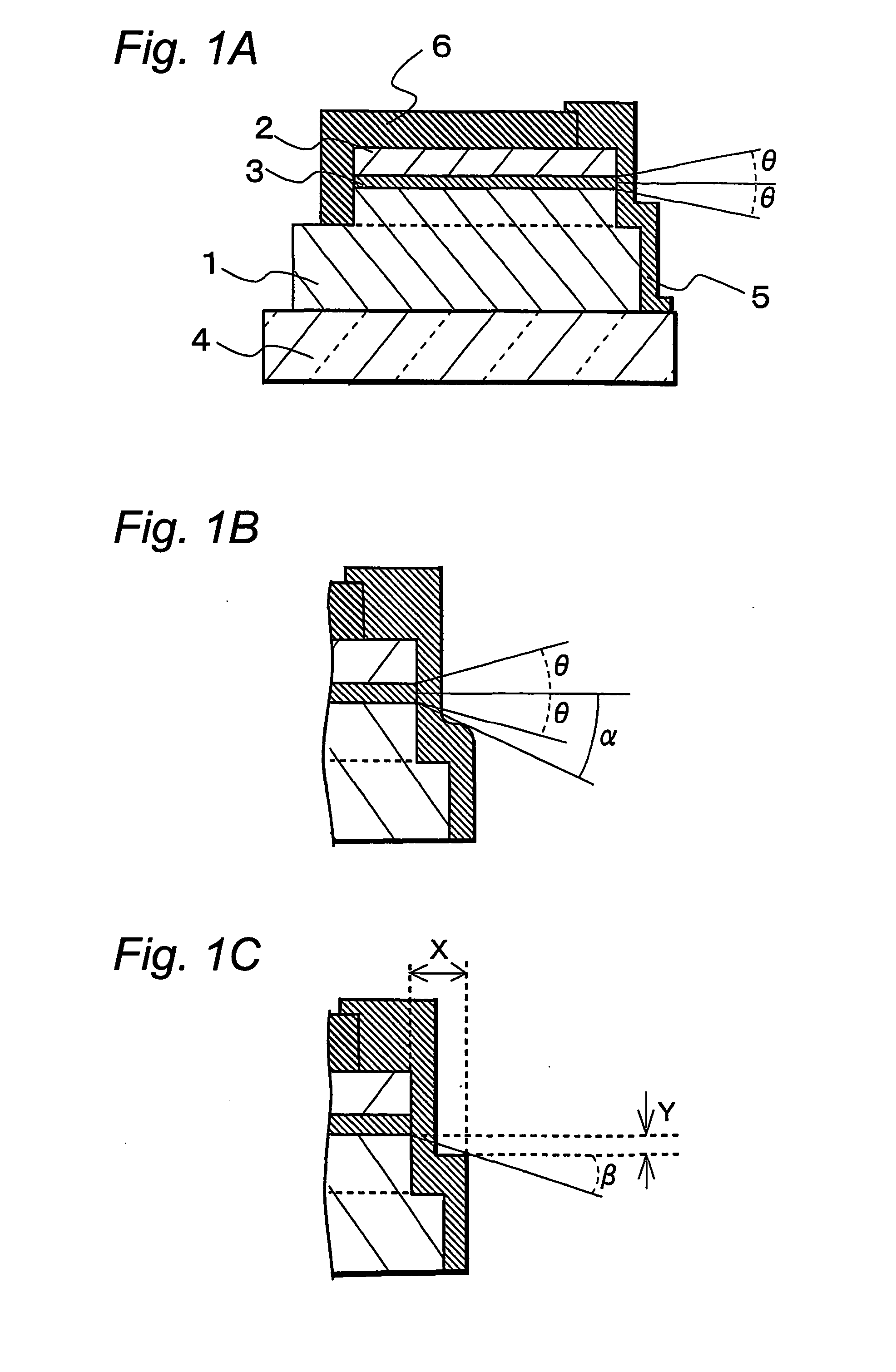
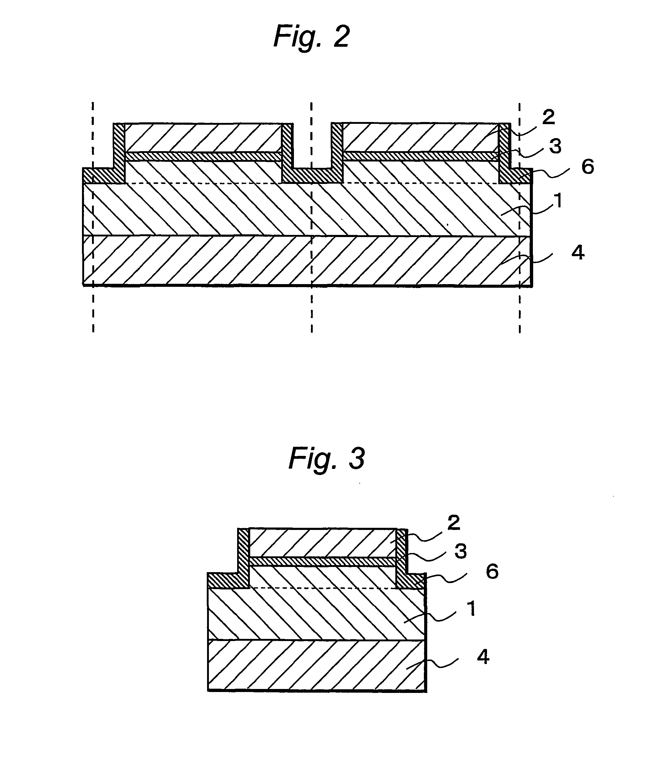
[0081] A laser device of a structure as shown in FIG. 1A using a nitride semiconductor is hereafter described. Example 1 uses a hetero substrate of a material different from the nitride semiconductor. The hetero substrate may be of a material different from the nitride semiconductor which material has been known to be able to grow the nitride semiconductor thereon, for example, an insulating substrate such as of sapphire with C plane, R plane or A plane as the principle plane and spinel (MgAl.sub.2O.sub.4), SiC (including 6H, 4H and 3C), ZnS, ZnO, GaAs, Si, an oxide substrate that lattice-matches with nitride semiconductors and the like. As preferable hetero substrates, may be mentioned sapphire and spinel. The hetero substrate may be off-angled, and in this case, a stepwise off-angled substrate is preferable because a base layer of gallium nitride can grow with good crystallinity. Further, in the case where the hetero substrate is used, after the nitride semiconductor is grown as t...

example 2

[0132] In Example 2, on the emission side, the protective film on the resonator face and the protective film on the end face of the projection are formed by separate steps. By thus forming through separate steps the protective films to be formed on end faces facing in the same direction, the protective film on the end face of the projection can be formed to have a different function from that of the protective film on the resonator face.

[0133] For forming such protective films, in Example 2, the protective film is formed on the resonator face on the emission side before the second end-face etch step in which etching is performed until the exposure of the substrate, while in Example 1 the protective film is formed continuously from the resonator face to the end face of the projection on the emission side after the second etch step.

[0134] The same process as in Example 1 is carried out before the protective film on the reflection side is formed of a dielectric multilayer film composed...

example 3

[0136] In Example 3, the protective film on the emission side is not formed to reach the substrate. In the second etch step in Example 1, etching is stopped to such an extent that the base layer formed on the sapphire substrate is exposed. The later steps are performed in the same manner as in Example 1. Thereby, in the last chip formation step, the semiconductor laser device of the invention is completed by dividing the sapphire substrate and the semiconductor layer. It is confirmed that the obtained semiconductor laser device continuously oscillates at an oscillation wavelength of 405 nm at a threshold current density of 20 kA / cm.sup.2 with a power of 30 mW at room temperature. A good beam is obtained in the FFP, especially in the emission full angle (19 to 34 degrees) of FFP-Y. The beam has an aspect ratio of 1.5. The beam exhibits satisfactory characteristics as light sources for optical disk systems. The laser device is free of shift of lateral transverse mode at an optical pow...


PUM


Abstract

A semiconductor laser device have, on a substrate, a semiconductor layer including an active layer sandwiched between an n-type layer and a p-type layer, the semiconductor layer having a sonator face formed by etching and a projection projecting out in an emission direction relatively to the resonator face, wherein a protective film is formed to extend from the resonator face to an end face of the projection, and, an emission critical angle, which is the largest angle at which light emitted from the resonator face can be radiated without being blocked by the projection and the protective film formed on the projection, is larger than an emission half-angle of an emission distribution in a vertical direction of a laser beam emitted from the resonator face.

Description

[0001] The present invention relates to a semiconductor laser device having a resonator face formed by etching, particularly to a semiconductor laser device using a group III-V nitride semiconductor such as GaN, AlN, InN or mixed crystal thereof (In.sub.bAl.sub.dGa.sub.1-b-dN, 0.ltoreq.b, 0 .ltoreq.d, b+d<1) and its manufacturing method.TECHNICAL BACKGROUND[0002] Today, there is an increasing demand for the use of semiconductor laser devices using nitride semiconductors for large-capacity high-density optical disk systems which are capable of recording and reproducing a large volume of data such as DVDs. For this reason, enthusiastic study is being done on semiconductor laser devices using nitride semiconductors. The semiconductor laser devices using nitride semiconductors are considered to be capable of oscillating and emitting a wide range from the ultraviolet region to visible wavelengths including the red region of, and they are expected to have a wide range of application in...

Claims


Application Information

Patent Timeline
Patent Type & Authority Applications(United States)
IPC IPC(8): H01S5/02H01S5/028H01S5/10
CPCH01S5/0203H01S5/028H01S5/0282H01S5/0286H01S5/1082H01S2301/18H01S5/323
Inventor FURUKAWA, YOSHIHIKOSHIMADA, MAKOTOKINOUCHI, AKIYOSHIOCHIAI, MASANAOSENOH, MASAYUKI
Owner NICHIA CORP
Why Eureka
Try Eureka