Semiconductor package and method of manufacturing the same which reduces warpage

a technology of semiconductor packaging and warpage reduction, which is applied in the direction of semiconductor/solid-state device details, semiconductor devices, electrical apparatus, etc., can solve the problems of warpage of semiconductor packaging, coefficients of thermal expansion, and difficulty in properly mounting the semiconductor package on the external devi

Inactive Publication Date: 2006-05-09
AMKOR TECH SINGAPORE HLDG PTE LTD
View PDF39 Cites 206 Cited by
  • Summary
  • Abstract
  • Description
  • Claims
  • Application Information

AI Technical Summary

Problems solved by technology

In the PMC or reflow process, when the semiconductor package is cooled down after heating, a warpage occurs in the semiconductor package due to a heat expansion coefficient difference between the semiconductor die and the encapsulant.
The difference in the coefficients of thermal expansion brings about a warpage due to th

Method used


Image

  • Semiconductor package and method of manufacturing the same which reduces warpage
  • Semiconductor package and method of manufacturing the same which reduces warpage
  • Semiconductor package and method of manufacturing the same which reduces warpage

Examples


Embodiment Construction

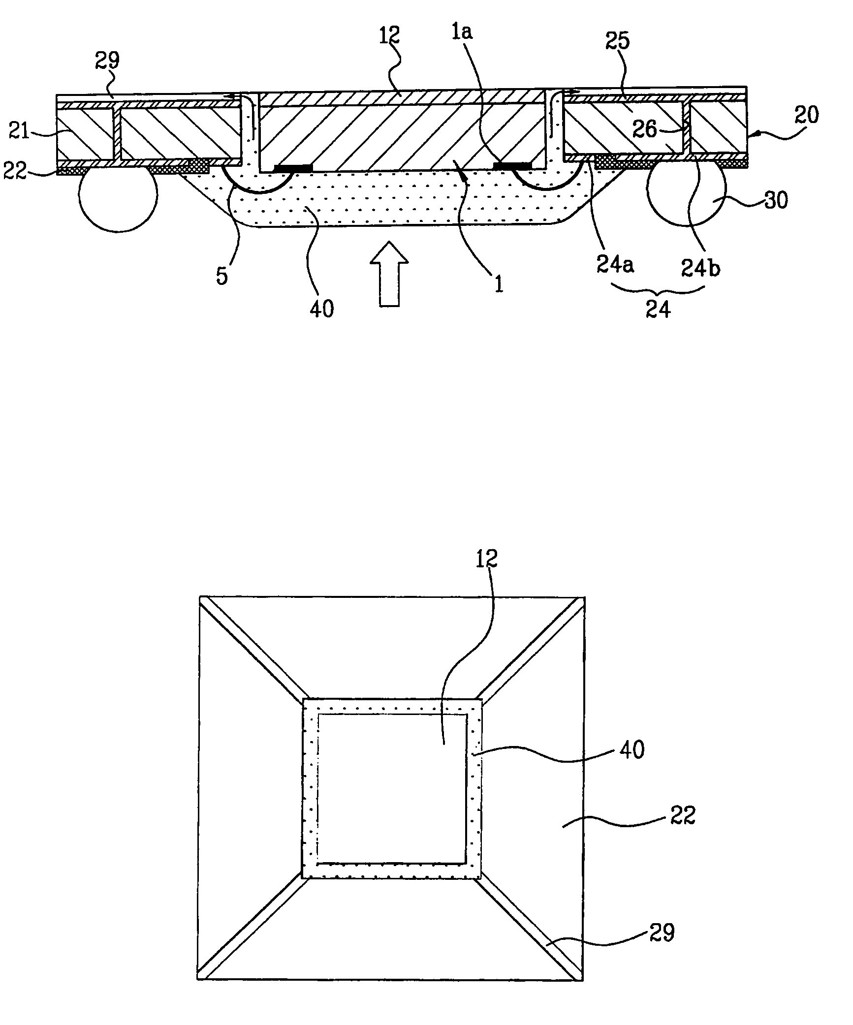
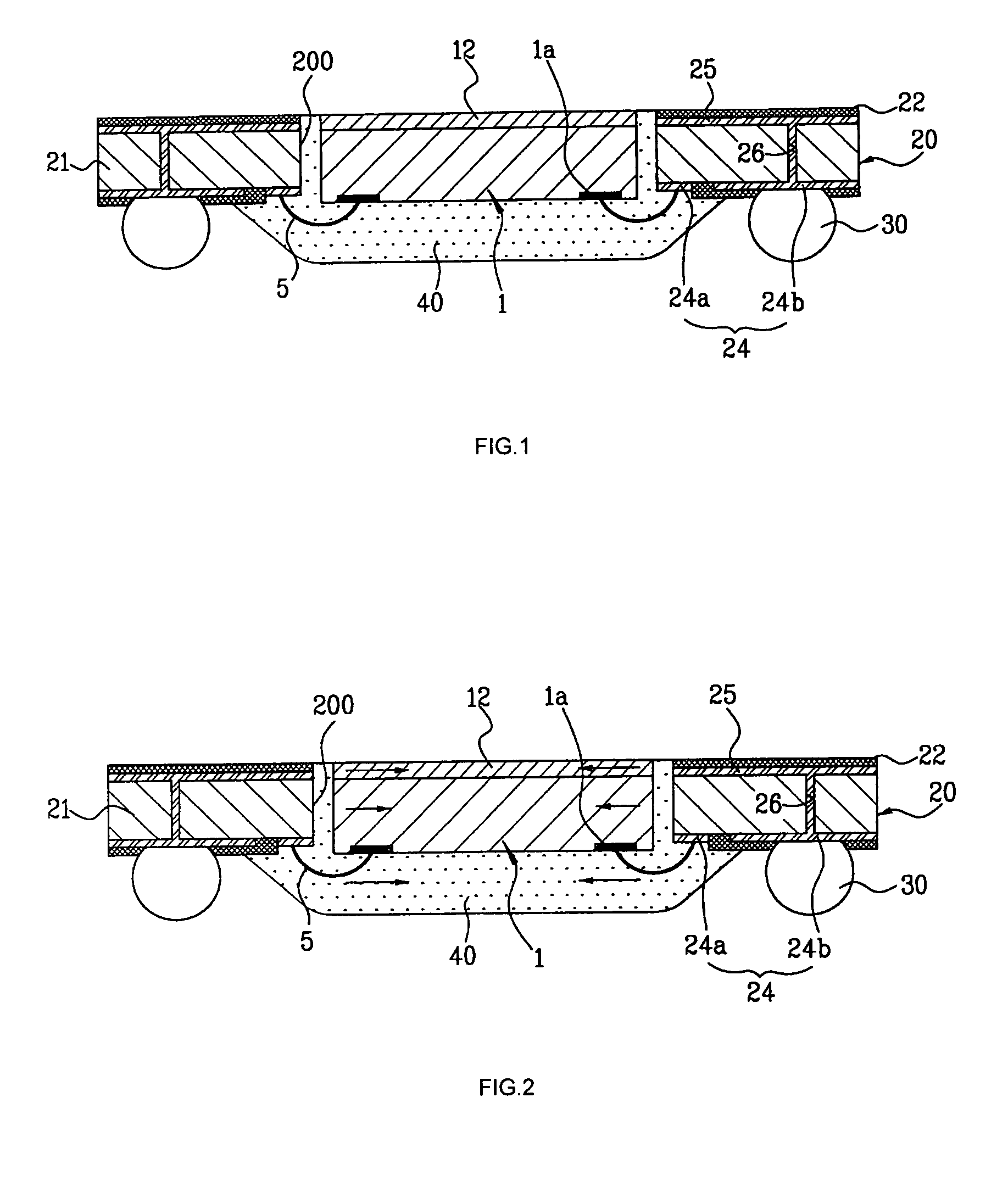
[0018]Referring to FIG. 1, a cross-sectional view of one embodiment of a semiconductor package according to the present invention is illustrated.

[0019]As shown in FIG. 1, a semiconductor package includes a semiconductor die 1. On a surface opposite to a integrated circuit forming face is a coating material 12. A cavity 200 is formed in a substrate 20. The cavity 200 is where the semiconductor die 1 is placed. An encapsulant 40 is used to encapsulate the integrated circuit forming face of the semiconductor die 1 lying in the cavity 200. Electrically conductive wire 5 are used to connect electrically the semiconductor die 1 to the substrate 20 for signal transfer between the semiconductor die 1 and substrate 20.

[0020]The semiconductor die 1 has bond pads 1a located so as to leave a predetermined interval from an inner face of the cavity 200 in the substrate 20.

[0021]There are various forms for the substrate 20 used for the semiconductor package. The substrate 20 may be printed circuit...


PUM


Abstract

A semiconductor package and method of producing the same has a semiconductor die having a first face and a second face. A coating material is coupled to the second face of the semiconductor die. A substrate having a cavity is provided wherein the semiconductor die is placed within the cavity. An encapsulant is used to encapsulate the second face of the semiconductor die placed in the cavity. Connection members are provided to couple the semiconductor die and the substrate in order to transfer signals between the semiconductor die and the substrate. Terminal members are couple to the substrate to connect the semiconductor package to an external device. In the semiconductor package, a thermal expansion coefficient of the coating material C and a thermal expansion coefficient of the encapsulant E should be approximately equal in value in order to limit the problems associated with warpage.

Description

FIELD OF THE INVENTION[0001]This invention relates to semiconductor devices and, more specifically, to a semiconductor package and method of manufacturing the same which reduces warpage during the cool down phase of the manufacturing process.BACKGROUND OF THE INVENTION[0002]In general, a semiconductor package is fabricated using a substrate such as lead frame, printed circuit board, circuit film, circuit tape, or the like. A semiconductor die is coupled to the substrate and packaged to be airtight to protected the semiconductor die from the outer environment as well as to enable the semiconductor package to be electrically connected to external devices.[0003]Namely, each semiconductor package has the structure enabling the semiconductor package to protect the semiconductor die as well as to be mounted on an external device, for example a mother board, or the like. In order to complete such a structure, processes of various steps are required.[0004]Generally speaking, there is Post M...

Claims


Application Information

Patent Timeline
IPC IPC(8): H01L23/02H01L21/44
CPCH01L23/13H01L23/3128H01L23/49816H01L2224/48091H01L2224/48227H01L2224/85001H01L24/48H01L2924/01079H01L2924/15311H01L2924/1532H01L2924/18165H01L2924/01078H01L2924/00014H01L2924/14H01L2924/181H01L2924/00H01L2924/00012H01L2224/45099H01L2224/45015H01L2924/207
Inventor KIM, YOUNG HOCHOI, SEOK HYUNLEE, CHOON HEUNGPARK, SUNG SUPARK, SUNG SOON
Owner AMKOR TECH SINGAPORE HLDG PTE LTD
Why Eureka
Try Eureka