Device and method for fabricating double-sided SOI wafer scale package with through via connections

a technology of soi wafers and scales, applied in the direction of semiconductor devices, semiconductor/solid-state device details, electrical apparatus, etc., can solve the problem of often not cost-effective integration of many different chips on a packag

Active Publication Date: 2006-05-18
GLOBALFOUNDRIES US INC
View PDF10 Cites 209 Cited by
  • Summary
  • Abstract
  • Description
  • Claims
  • Application Information

AI Technical Summary

Problems solved by technology

The integration of many different chips on a package is often not co...

Method used


Image

  • Device and method for fabricating double-sided SOI wafer scale package with through via connections
  • Device and method for fabricating double-sided SOI wafer scale package with through via connections
  • Device and method for fabricating double-sided SOI wafer scale package with through via connections

Examples


Embodiment Construction

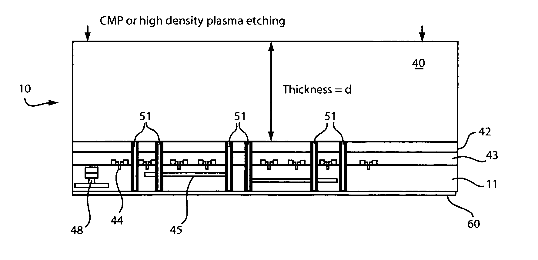
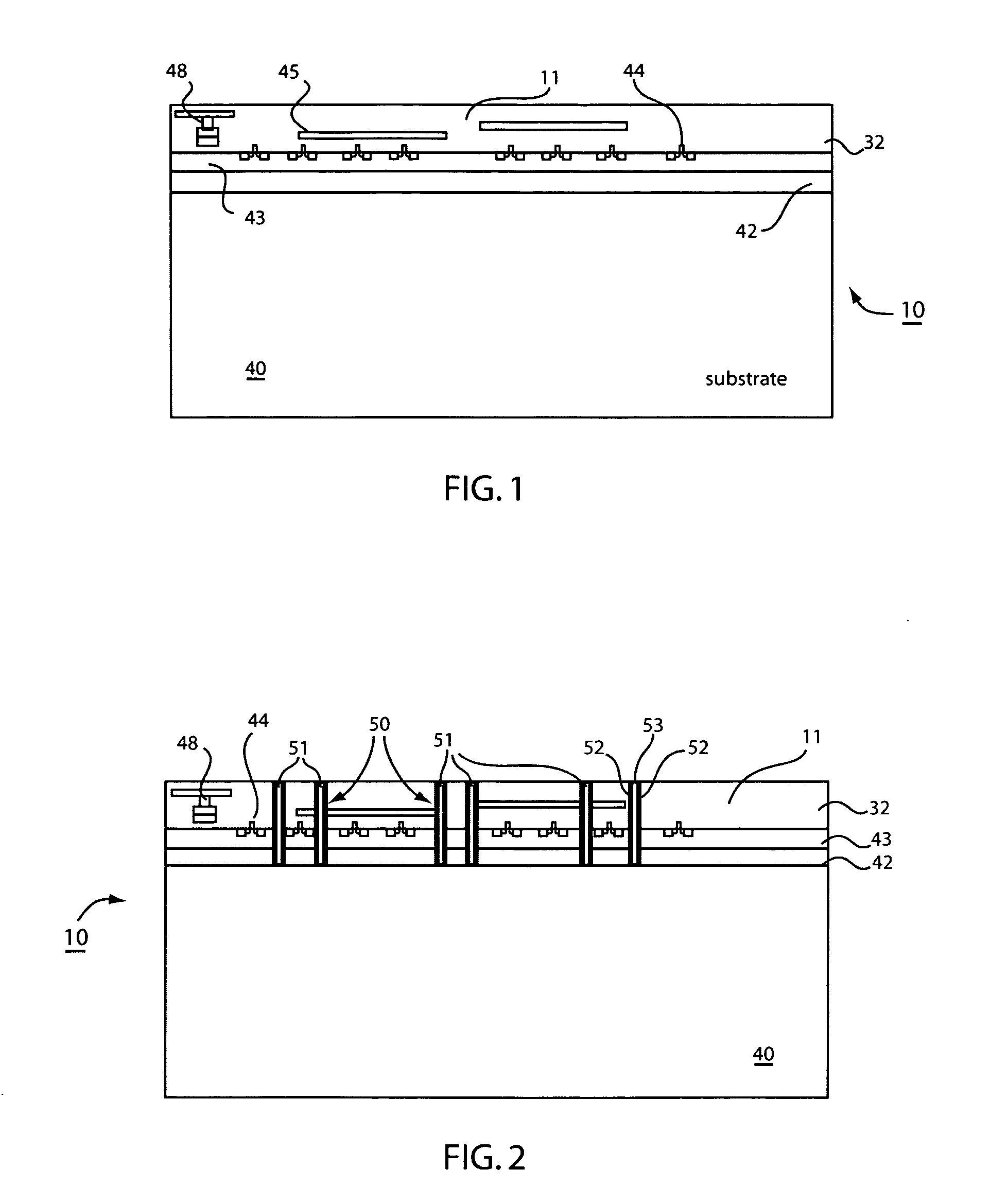
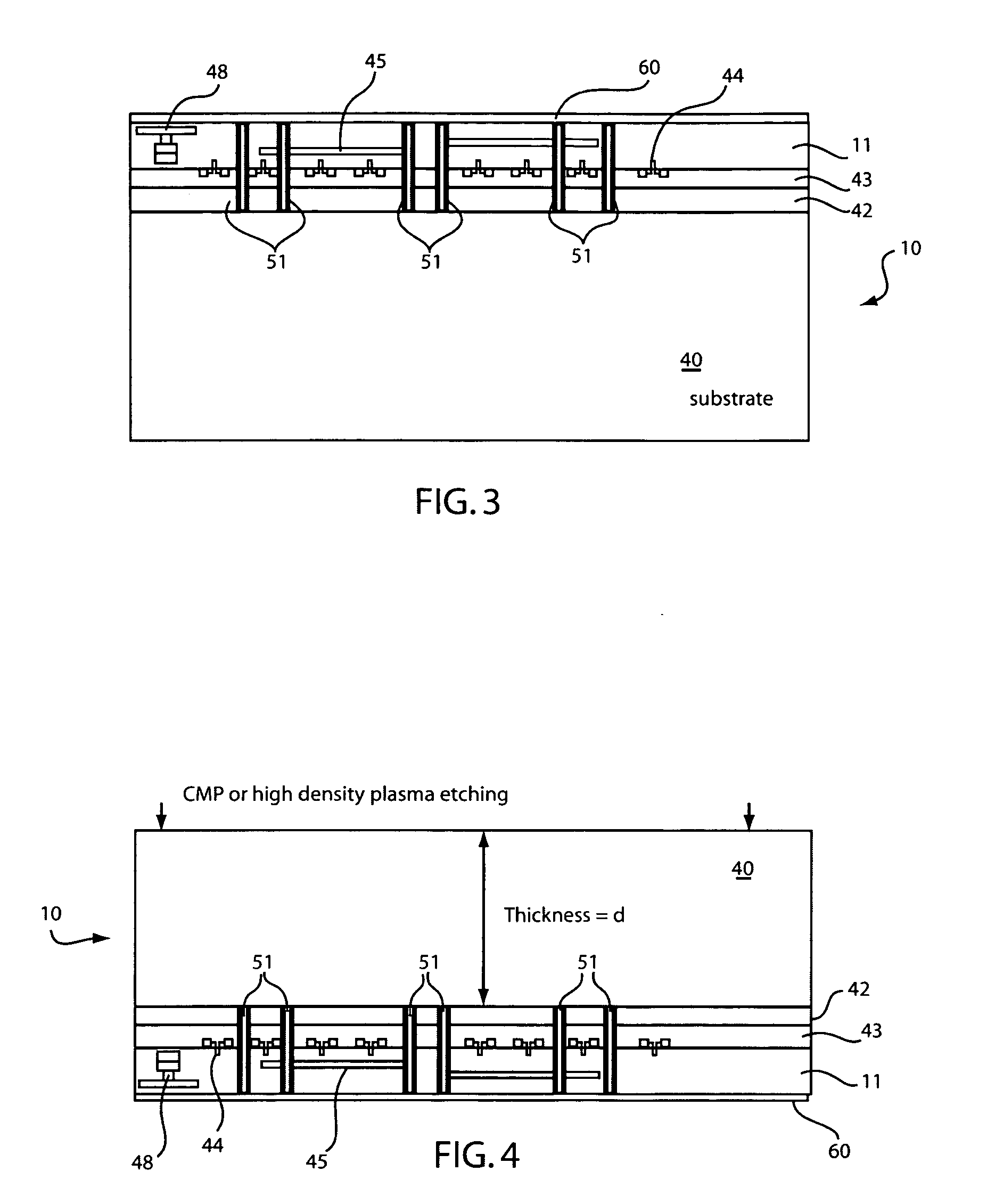
[0032] The present invention provides a low-cost and high-yield double-sided wafer scale package preferably on a silicon-on-insulator (SOI) wafer. A mother chip is formed on the front side of the SOI wafer with a fully or partially depleted body to achieve high performance. A plurality of thinned daughter chips are then mounted inside the cavities on the backside of the SOI wafer, opposite the mother chip. Through silicon and buried oxide, metal studs are fabricated to facilitate interconnection between the mother and daughter chips.

[0033] Advantageously, the present methods do not need the chips to be transferred from a temporary carrier to a permanent carrier, which reduces the cost. In accordance with this disclosure, by employing through via connections and cavity formation, sub-chips (daughter chips) can be directly diced out of a wafer and mounted on the backside of the mother chip. The method further avoids the use of vertical stacking in a 3-D package to facilitate heat dis...


PUM


Abstract

A semiconductor package includes an SOI wafer having a first side including an integrated circuit system, and a second side, opposite the first side, forming at least one cavity. At least one chip or component is placed in the cavity. A through buried oxide via connects the chip(s) to the integrated circuit system.

Description

BACKGROUND OF THE INVENTION [0001] 1. Field of the Invention [0002] The present invention relates to semiconductor processing and devices, and more particularly to devices and methods, which employ silicon-on-insulator (SOI) technology to provide a double-sided chip structure. [0003] 2. Description of the Related Art [0004] As the relentless scaling of complementary metal oxide semiconductor (CMOS) technology approaches its physical limit, the integration of very large-scale integrated circuit (VLSI) systems on a package (SoP) becomes increasingly important. The integration of many different chips on a package is often not cost effective, due to the incompatibility between various chip technologies. For example, non-volatile random access memory (NVRAM) with floating gate devices and dynamic random access memory (DRAM) with deep trenches require additional masks and processing steps to fabricate. High-speed Gallium Arsenide (GaAs) chips are manufactured on a different substrate than...

Claims


Application Information

Patent Timeline
IPC IPC(8): H01L21/44
CPCH01L21/76898H01L23/481H01L2924/1461H01L2924/10253H01L2924/13091H01L25/0652H01L25/18H01L2221/68345H01L2221/68363H01L2224/16H01L2924/01078H01L2924/01079H01L2924/15153H01L2924/1517H01L2924/16195H01L2924/00H01L24/05H01L24/94H01L2224/05009H01L2224/0557H01L2224/06181H01L2224/14181H01L2224/16146H01L2224/81191H01L2224/81192H01L2224/94H01L2924/14H01L2224/11H01L2224/81
Inventor CHEN, HOWARD HAOHSU, LOUIS LU-CHEN
Owner GLOBALFOUNDRIES US INC
Why Eureka
Try Eureka