Semiconductor device package integrated with coil for wireless charging and electromagnetic interference shielding, and method of manufacturing the same

a technology of electromagnetic interference shielding and semiconductor devices, applied in the direction of magnetic materials, magnetic bodies, transportation and packaging, etc., can solve the problems of reducing the level of emissions that can pass through the casing, adversely affecting the operation of the semiconductor device, and progressively more complex semiconductor devices

Active Publication Date: 2016-10-04
ADVANCED SEMICON ENG INC
View PDF8 Cites 207 Cited by
  • Summary
  • Abstract
  • Description
  • Claims
  • Application Information

AI Technical Summary

Problems solved by technology

Semiconductor devices have become progressively more complex, driven at least in part by the demand for enhanced processing speeds and smaller sizes.
While the benefits of enhanced processing speeds and smaller sizes are apparent, these characteristics of semiconductor devices also can create problems.
If the level of electromagnetic emissions at a neighboring semiconductor device is sufficiently high, these emissions can adversely affect the operation of that semiconductor device.
When elect

Method used


Image

  • Semiconductor device package integrated with coil for wireless charging and electromagnetic interference shielding, and method of manufacturing the same
  • Semiconductor device package integrated with coil for wireless charging and electromagnetic interference shielding, and method of manufacturing the same
  • Semiconductor device package integrated with coil for wireless charging and electromagnetic interference shielding, and method of manufacturing the same

Examples


Embodiment Construction

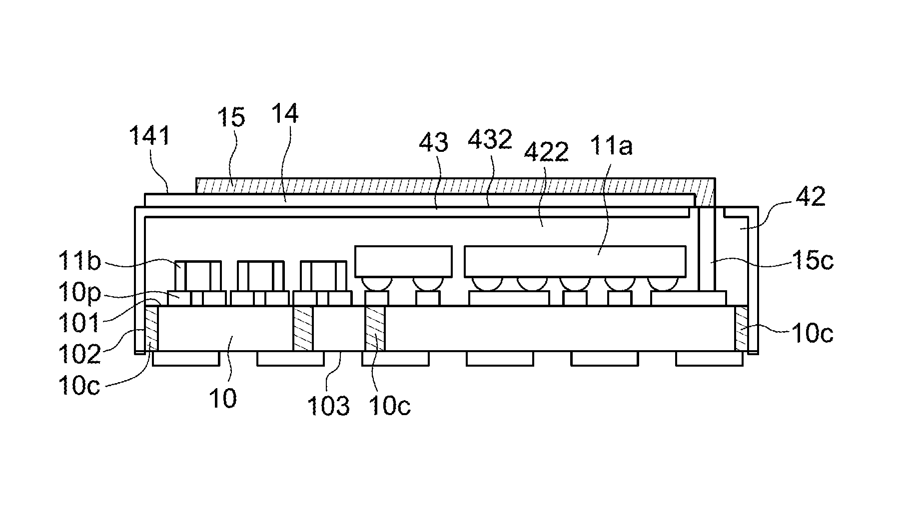
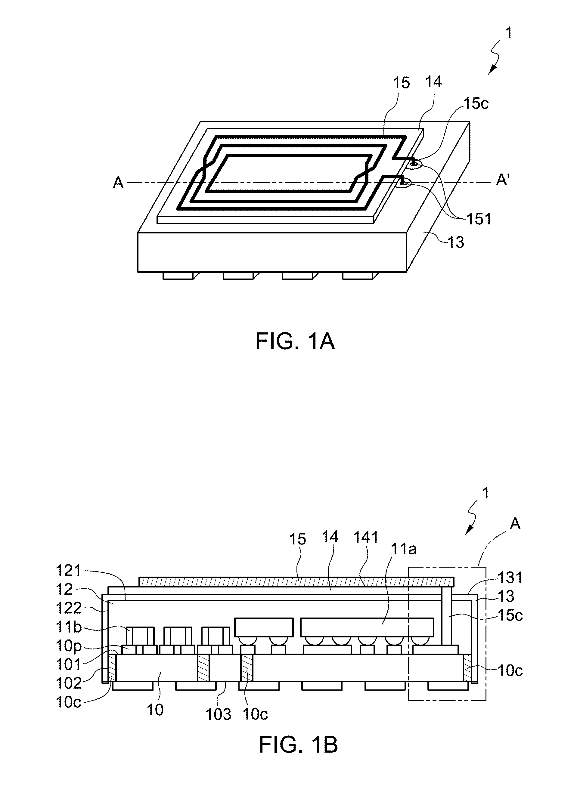
[0017]FIG. 1A illustrates a top view of a semiconductor device package 1 in accordance with an embodiment of the present disclosure. The semiconductor device package 1 includes an EMI shield 13 covering a substrate and electronic components (not shown), a magnetic insulating layer 14 and a patterned conductive layer 15.

[0018]The patterned conductive layer 15 includes at least two terminals 151, each of which electrically connects to a respective conductive element 15c. The patterned conductive layer 15 can be magnetically coupled to an external magnetic field, which induces a current in the conductive layer 15. An induced current can be transmitted to one or more electronic components covered by the EMI shield 13 through the conductive elements 15c. The patterned conductive layer 15 can be patterned in a shape suitable for a desired coupling to the external magnetic field. In one or more embodiments, the patterned conductive layer 15 is in a pattern of multiple concentric and overla...


PUM


Abstract

The present disclosure relates to a semiconductor device package which includes a carrier, an electronic component, conductive elements, a package body, a shield, a magnetic insulating layer, and a patterned conductive layer. The carrier has a top surface on which the electronic component is disposed. The conductive elements are disposed on the top surface of the carrier. The package body is disposed on the top surface of the carrier and encapsulates the electronic component and a portion of each of the conductive elements. The shield is disposed on the package body and covers an exterior of the package body. The magnetic insulating layer is disposed on a top surface of the shield. The patterned conductive layer is disposed on the magnetic insulating layer. Each of the conductive elements electrically connects the patterned conductive layer to the electronic component.

Description

BACKGROUND[0001]1. Technical Field[0002]The present disclosure relates generally to semiconductor device packages and the manufacturing methods thereof. More particularly, the present disclosure relates to semiconductor device packages integrated with coils for wireless charging and integrated with shields for electromagnetic interference shielding, and the manufacturing methods thereof.[0003]2. Description of the Related Art[0004]Semiconductor devices have become progressively more complex, driven at least in part by the demand for enhanced processing speeds and smaller sizes. While the benefits of enhanced processing speeds and smaller sizes are apparent, these characteristics of semiconductor devices also can create problems. In particular, higher clock speeds can involve more frequent transitions between signal levels, which, in turn, can lead to a higher level of electromagnetic emissions at higher frequencies or shorter wavelengths. Electromagnetic emissions can radiate from a...

Claims


Application Information

Patent Timeline
IPC IPC(8): H01L23/552H01L21/768H01L21/26H01L21/52H01L23/538H01L23/31H01L23/04H02J7/02H01L21/56H01L21/48H01L23/64
CPCH01L23/552H01L21/76892H01L23/5386H01L23/04H01L23/645H01L21/52H01L21/4817H01L21/56H01L23/3107H02J7/025H01L24/13H01L24/16H01L24/48H01L2224/13147H01L2224/16227H01L2224/16235H01L2224/48227H01L2924/15313H01L2924/1815H01L2924/19041H01L2924/19042H01L2924/19043H01L2924/19105H01L2924/3025H01L2924/00014H01L2924/181H01L25/16H01L2224/45015H01L2924/207H01L2224/45099H01L2924/00H01F1/00H02J50/10H01L21/485H01L21/4853H01L21/486H01L21/565H01L23/3114H01L23/49811H01L23/49827H01L23/49838H01L25/0655
Inventor TSAI, MING-HORNGCHEN, WEI-YULEE, CHUN-CHIALI, HUAN WUN
Owner ADVANCED SEMICON ENG INC
Why Eureka
Try Eureka