

Circuit board for direct flip chip attachment
a circuit board and chip technology, applied in the field of electric and electronic arts, can solve the problems of increased packaging complexity and concomitant yield reduction, introduction of additional thermal resistance, and possible incompatibility between the submount material and processing operations performed,
- Summary
- Abstract
- Description
- Claims
- Application Information
AI Technical Summary
Benefits of technology
Problems solved by technology
Method used
Image

Examples
Embodiment Construction
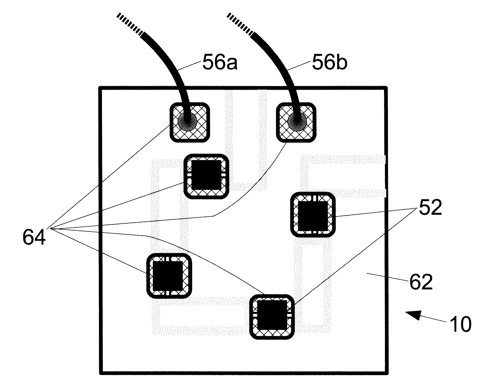
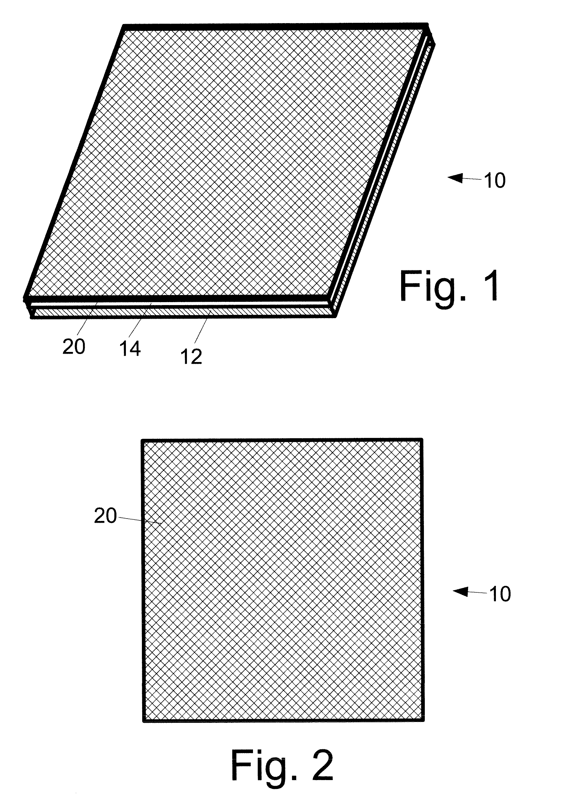
[0019]FIGS. 1 and 2 show perspective and top views of a circuit board 10 which includes a relatively thick metal substrate 12 on which is disposed a relatively thin electrically insulating layer 14, on top of which is disposed an electrically conductive layer 20 made of copper, a copper alloy, or another suitable electrically conductive material. The electrically conductive layer 20 is intended to be patterned by spatially selective removal to define electrically conductive circuitry for interconnecting one or more electronic components to be mounted on the circuit board 10.
[0020]The circuit board 10 is of the type sometimes referred to as a metal core printed circuit board, where the term “metal core” refers to the relatively thick metal substrate 12. In such circuit boards, the metal core 12 is intended to provide both mechanical support and also thermal heat spreading or heat sinking. The electrically insulating layer 14 is relatively thin in order to provide good thermal transfe...
PUM
 Abstract
Description
Claims
Application Information