Supercharge Your Innovation With Domain-Expert AI Agents!

FOUP and automated wafer transfer system

A wafer transfer box and wafer technology, applied in the direction of conveyor objects, transportation and packaging, electrical components, etc., can solve the problems of wafer pollution, wafer transfer box cannot be closed and opened automatically, and achieve the effect of avoiding pollution

Active Publication Date: 2020-07-14
SHANGHAI MICRO ELECTRONICS EQUIP (GRP) CO LTD
View PDF6 Cites 0 Cited by
  • Summary
  • Abstract
  • Description
  • Claims
  • Application Information

AI Technical Summary

Problems solved by technology

[0004] The purpose of the present invention is to provide a wafer transfer box and an automatic wafer transfer system to solve the problem that the wafer is contaminated during the transfer process and the wafer transfer box cannot be automatically closed and opened

Method used


Image

  • FOUP and automated wafer transfer system
  • FOUP and automated wafer transfer system
  • FOUP and automated wafer transfer system

Examples


Embodiment 1

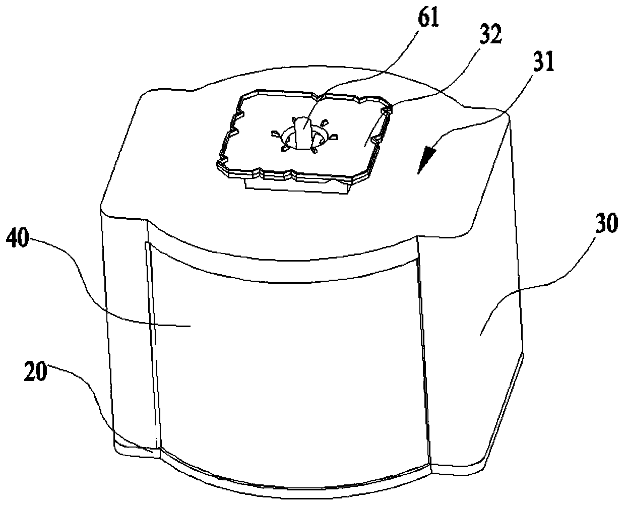
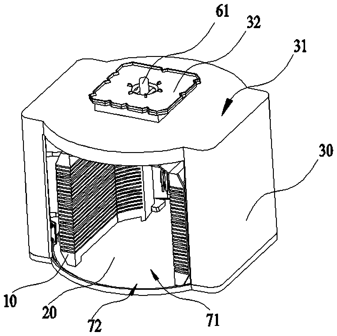
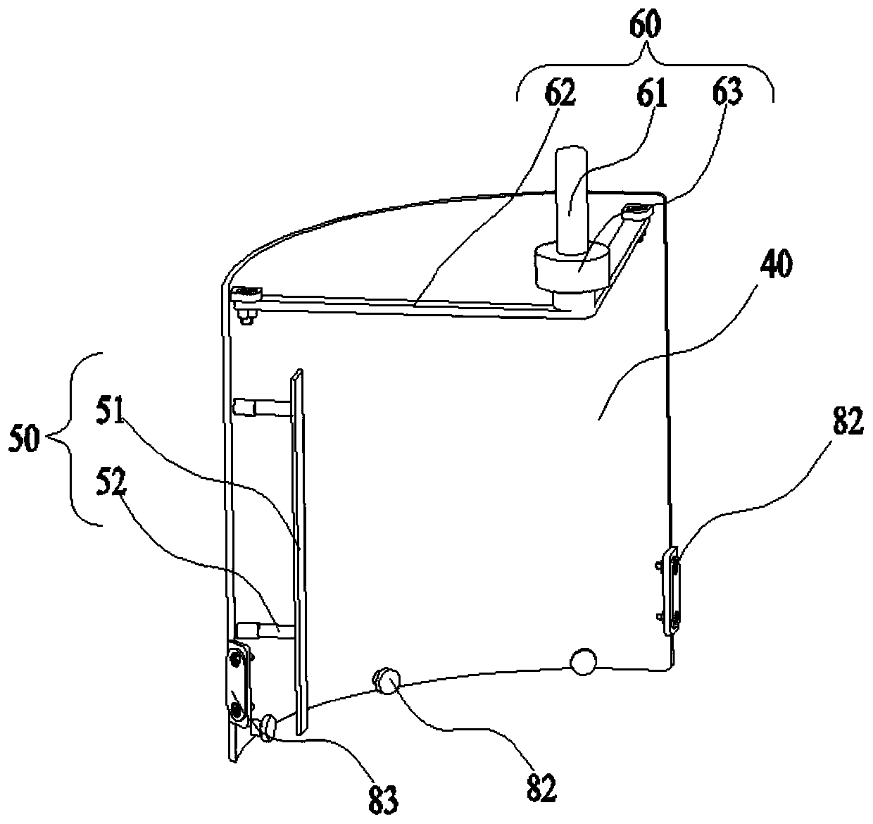
[0056] figure 1 It is a structural schematic diagram of the FOUP in an embodiment of the present invention when the box cover is in a closed state, figure 2 It is a structural schematic diagram of the FOUP in an embodiment of the present invention when the box cover is in an open state. refer to figure 1 and figure 2 , the wafer transfer box includes a wafer storage frame 10, a base 20, a cover 30, a lid 40 and a rotary connection mechanism 60 ( figure 1 and figure 2 not shown). The wafer storage frame 10 is used for storing wafers. The base 20 and the cover 30 are fixedly connected, and the base 20 and the cover 30 enclose a cavity 71 for accommodating the wafer storage frame 10 . The cover 30 is provided with an opening 72 for picking and placing wafers. The box cover 40 is rotatably connected to the housing 30 through the rotary connection mechanism 60 , and when the rotary connection mechanism 60 is rotated, the box cover 40 slides on the base 20 to close and ope...

Embodiment 2

[0082] Different from Example 1, as Figure 6 As shown, the frame positioning mechanism in this embodiment is a frame positioning protrusion 332, and the frame positioning protrusion 332 can be connected with the bottom of the wafer storage frame 10 to limit the position of the wafer storage frame 10. role.

[0083]Optionally, the automatic wafer transfer system using the FOUP described in Embodiment 2 also includes a FOUP platform, and the carrying surface of the FOUP is connected to the lower surface of the base 20 of the FOUP. The surface can be limitedly connected, specifically, a positioning platform 34 is set on the lower surface of the base 20, such as Figure 7 As shown, correspondingly, a positioning seat matching the positioning platform is provided on the carrying surface of the wafer cassette carrier, and vice versa.

[0084] The wafer transport box of the present invention can be used to transport wafers of various specifications, including but not limited to 8 ...


PUM


Abstract

The invention provides a wafer transfer box and a wafer automatic transfer system, which include a wafer storage frame for storing wafers, a base, a cover, a box cover and a rotary connection mechanism. The base and the cover are fixedly connected, and the base and the cover enclose a cavity for accommodating the wafer storage frame, and the cover is provided with a An opening, the box cover is rotatably connected to the casing through the rotary connection mechanism, and when the rotary connection mechanism is rotated, the box cover slides on the base to close and open the opening. In the present invention, by placing the wafer storage frame for storing wafers in the cavity surrounded by the base and the cover, the wafers are prevented from being polluted during transmission; The trajectory moves to close the box cover and open the opening, realizing the automatic closing and opening of the FOUP.

Description

technical field [0001] The invention relates to the technical field of microelectronic processing, in particular to a wafer transfer box and an automatic wafer transfer system. Background technique [0002] Currently, integrated circuits are widely used in electronic products, such as computers, industrial control equipment, and consumer electronics. With the rapid development of electronic products, technologies such as IC design and integrated circuit manufacturing are also developing rapidly. Various devices in integrated circuits are mostly fabricated on wafers. [0003] In the manufacturing process of integrated circuits, any particles, such as particles, dust, organic matter, etc., can easily contaminate the wafer and cause defects in the wafer, thereby affecting the quality of integrated circuits. Therefore, integrated circuits need to be produced in a clean environment . Most of the wafers carried by the wafer storage frame are in a bare state. If the cleanliness ...

Claims


Application Information

Patent Timeline
Patent Type & Authority Patents(China)
IPC IPC(8): H01L21/677
CPCH01L21/6773H01L21/67772H01L21/67379H01L21/67373H01L21/67386H01L21/677
Inventor 甄静许琦欣王刚章力龙欣江陈西平
Owner SHANGHAI MICRO ELECTRONICS EQUIP (GRP) CO LTD
Features
  • R&D
  • Intellectual Property
  • Life Sciences
  • Materials
  • Tech Scout
  • Unparalleled Data Quality
  • Higher Quality Content
  • 60% Fewer Hallucinations
Learn More