Method for fabricating semiconductor chip

a semiconductor chip and fabrication method technology, applied in the direction of manufacturing tools, solid-state devices, welding/soldering/cutting articles, etc., can solve the problems of insufficient bonding function of film, unrealistic affixing of semiconductor wafer before plasma dicing performance as described in patent document 2, and the inability to accurately shape the small piece of die attached film affixed to the minute semiconductor chip

Active Publication Date: 2010-08-03
PANASONIC CORP
View PDF20 Cites 180 Cited by
  • Summary
  • Abstract
  • Description
  • Claims
  • Application Information

AI Technical Summary

Benefits of technology

[0011]Accordingly, the present invention aims at providing a method for fabricating a semiconductor chip which enables achievement of both plasma dicing and bonding involving use of a die attach film and which enables prevention of contamination of the inside of a vacuum chamber for plasma processing.
[0020]The die attach film used as a mask in plasma etching is used, as it is, as an adhesive for a leadframe, a substrate, and the like, after removal of the heat-resistant film. Accordingly, a step of removal (ashing) of a resist film, which is indispensable for related-art plasma dicing, becomes unnecessary, and contamination of the inside of a vacuum chamber for plasma processing, which would otherwise be caused during the course of removal of a resist film, can be prevented.

Problems solved by technology

Incidentally, when a die attach film is exposed to a high-temperature environment which is at a temperature of 100° C. or higher, curing reaction usually proceeds, whereupon the film does not exhibit sufficient function as a bonding agent.
For this reason, affixing of a semiconductor wafer before performance of plasma dicing as described in Patent Document 2 is unrealistic.
However, accurately shaping the small piece of the die attach film affixed to the minute semiconductor chip is extremely difficult, and difficulty has been encountered in essentially attaining both plasma dicing and bonding involving use of a die attach film.
Moreover, plasma dicing also entails a problem of contamination of a vacuum chamber for plasma processing with organic compounds which arise during a process for ashing (incineration removal) of a resist film, and measures against the problem has been the urgent necessity.

Method used


Image

  • Method for fabricating semiconductor chip
  • Method for fabricating semiconductor chip
  • Method for fabricating semiconductor chip

Examples


Embodiment Construction

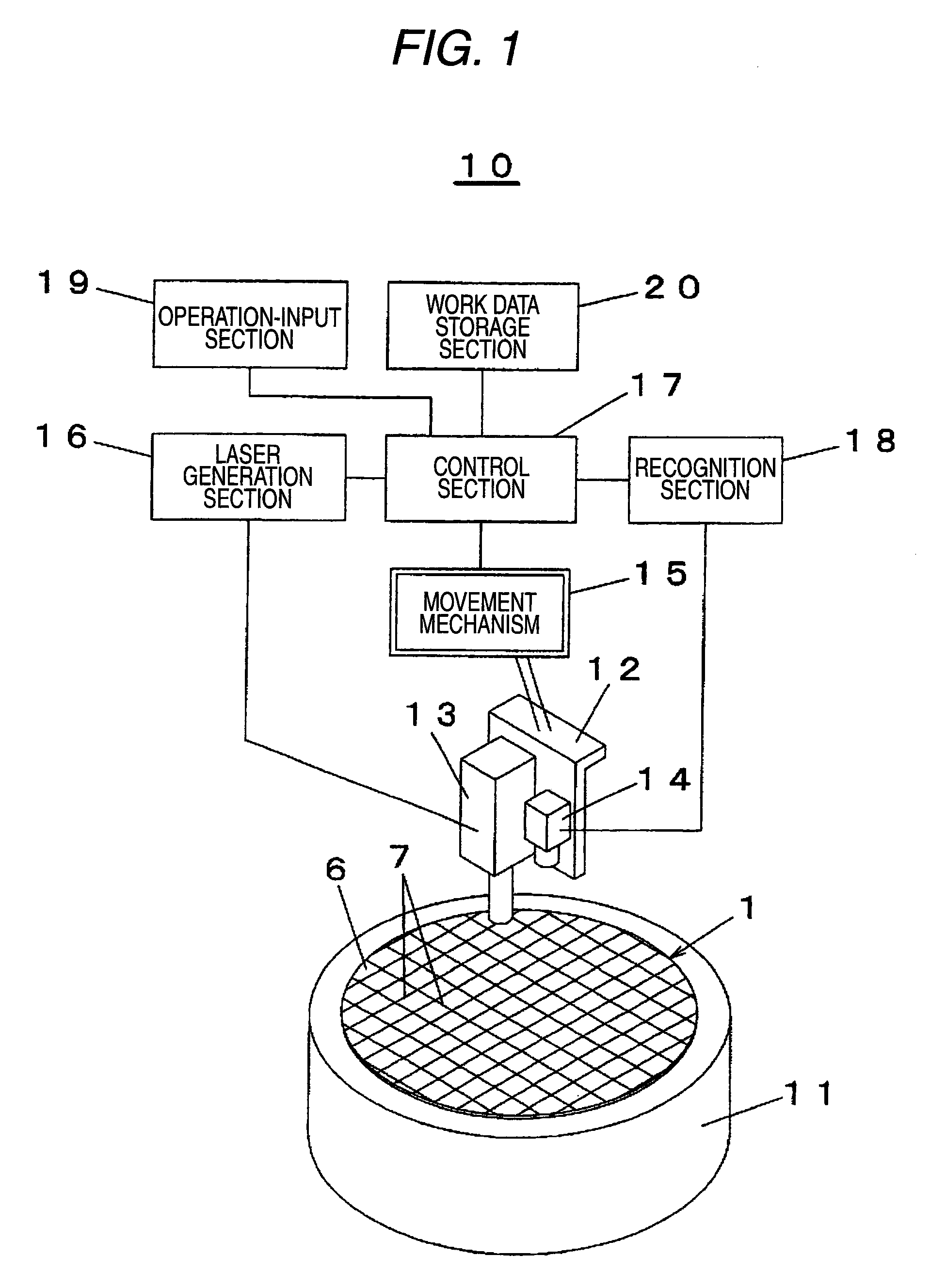
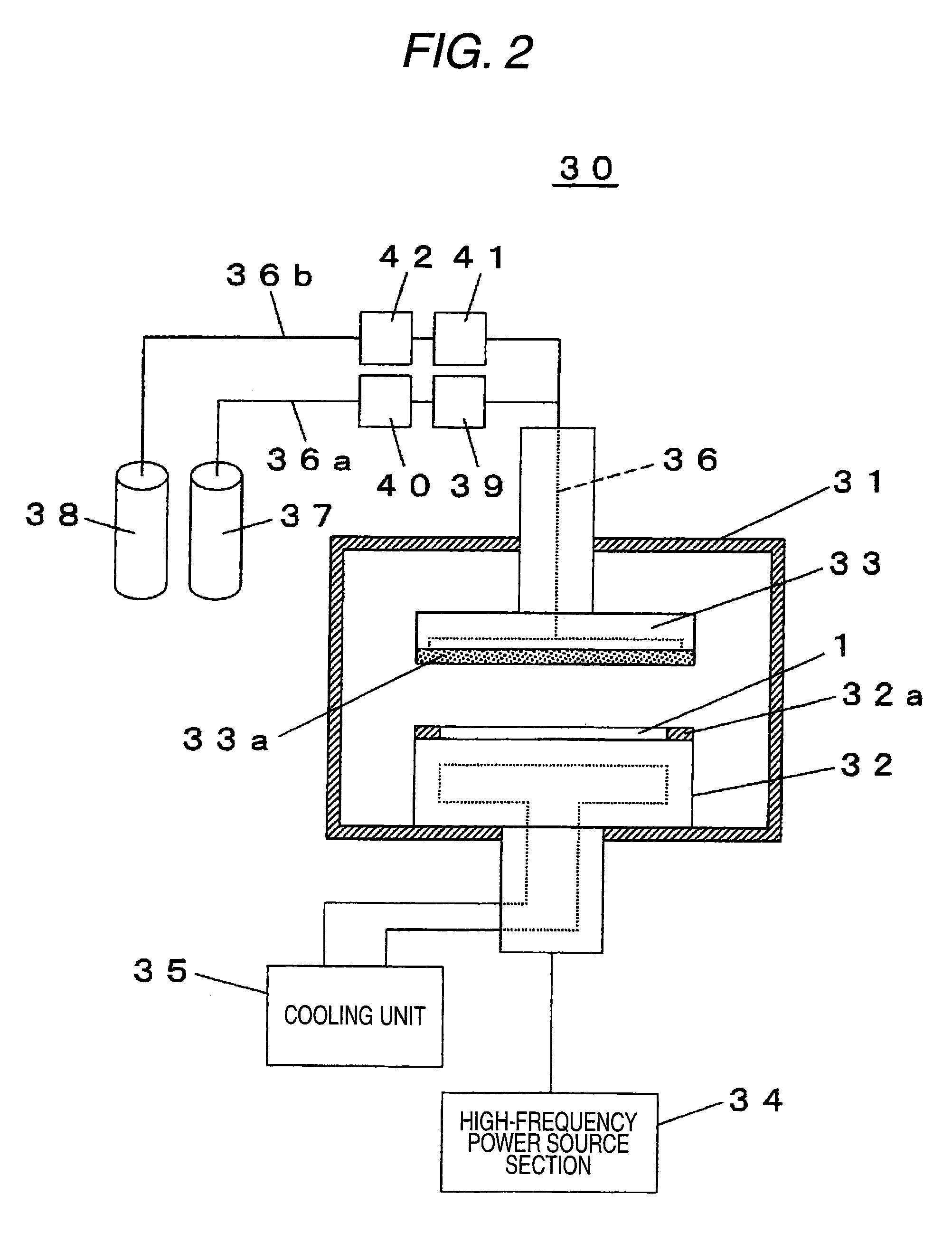
[0029]An embodiment of the present invention will be described hereunder by reference to the drawings. The configuration of a laser beam machining apparatus 10 and a plasma processing apparatus 30 used in implementation of the method for fabricating a semiconductor chip of an embodiment of the present invention will first be described by reference to FIGS. 1 and 2.

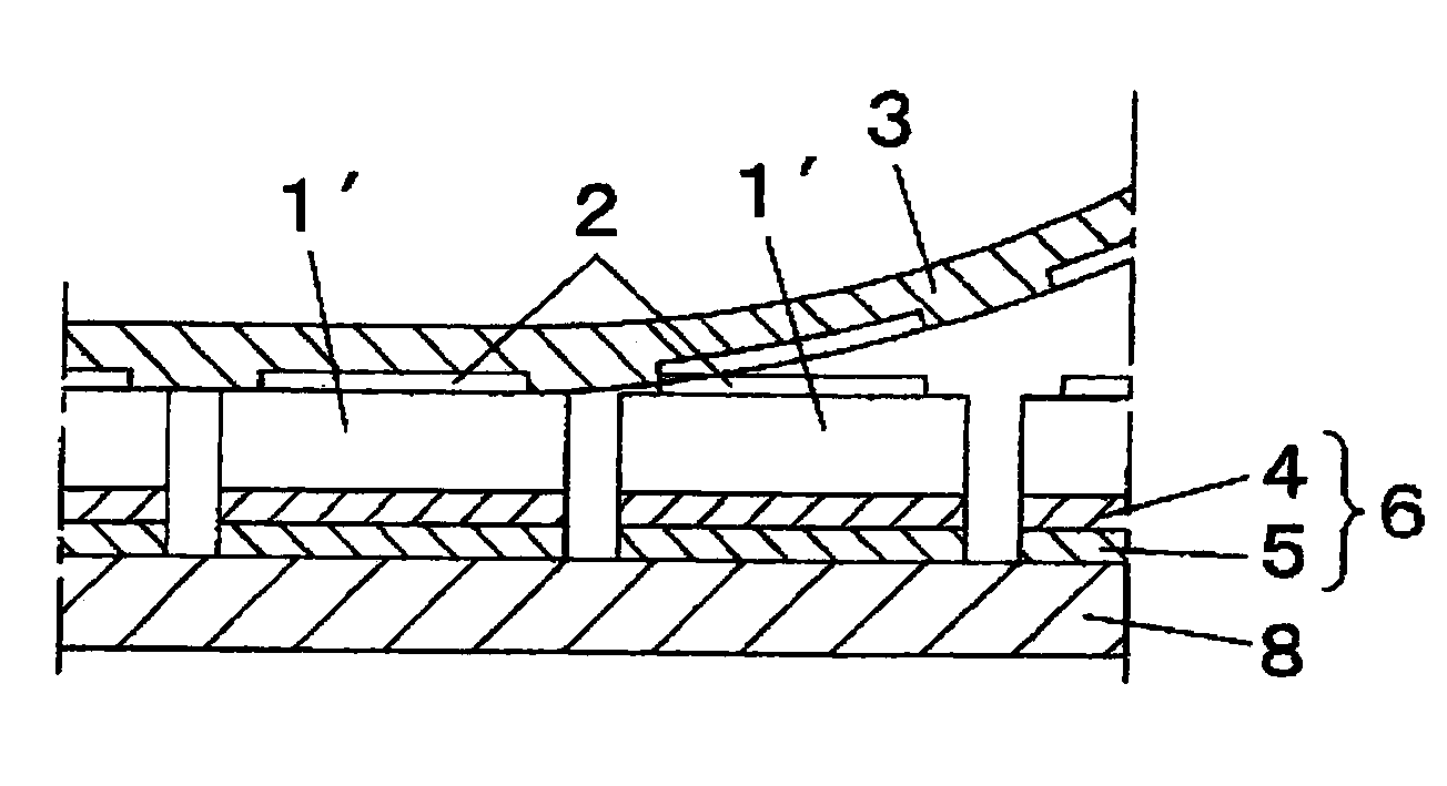
[0030]In FIG. 1, the laser beam machining apparatus 10 includes a wafer holding section 11 for holding in a level position a semiconductor wafer 1 which is an object of processing; a moving plate 12 provided in a movable manner at an elevated position above the wafer holding section 11; a laser emission section 13 and a camera 14 which are fixed to the moving plate 12; a movement mechanism 15 for moving the moving plate 12; a laser generation section 16 for causing the laser emission section 13 to generate a laser beam; a control section 17 for controlling driving of the movement mechanism 15 and generation of a laser beam...


PUM

PropertyMeasurementUnit
temperatureaaaaaaaaaa
thicknessaaaaaaaaaa
temperatureaaaaaaaaaa

Abstract

After a film layer 6 formed from a die attach film 4 and a UV tape 5 has been provided as a mask on a semiconductor wafer 1, boundary trenches 7 for partitioning semiconductor elements 2 formed on a circuit pattern formation surface 1a are formed in the film layer 6, thereby making a surface 1c of a semiconductor wafer 1 exposed. The exposed surface 1c of the semiconductor wafer 1 in the boundary trenches 7 is etched by means of plasma of a fluorine-based gas, and the semiconductor wafer 1 is sliced into semiconductor chips 1′ along the boundary trenches 7.

Description

TECHNICAL FIELD[0001]The present invention relates to a semiconductor chip fabrication method for fabricating semiconductor chips by slicing a semiconductor wafer through use of plasma dicing.BACKGROUND ART[0002]A related-art process for fabricating a semiconductor includes forming a plurality of semiconductor elements on a circuit pattern formation surface of a semiconductor wafer and subsequently slicing (cutting) the semiconductor wafer, in a mechanical manner, so as to separate the semiconductor elements from each other. A fabricated semiconductor chip is bonded to a leadframe, a substrate, and the like, by means of an epoxy-resin-based liquid adhesive. However, a film-shaped adhesive called a die attach film (DAF) which is easy to handle in connection with a thin semiconductor chip has recently been used.[0003]The die attach film is affixed to a rear surface of a semiconductor wafer (i.e., a surface opposite to a circuit pattern formation surface) before mechanical dicing of th...

Claims


Application Information

Patent Timeline
Patent Type & Authority Patents(United States)
IPC IPC(8): H01L21/00
CPCB23K26/4065H01L21/78H01L24/743H01L2224/743H01L2924/00B23K2103/42B23K2103/50H01L2924/12042H01L21/3065
Inventor ARITA, KIYOSHIHAJI, HIROSHI
Owner PANASONIC CORP
Why Eureka
Try Eureka