
A Tunable Waveguide System for Nanoscale Focusing of X-rays

An X-ray and nanoscale technology, which is applied in the field of particle or ionizing radiation processing devices, can solve the problems of fixed gaps that cannot accurately locate the focal length, differences, etc., and achieve the effect of compensating for the loss of focusing performance

Active Publication Date: 2020-10-02
深圳市柯尼达医疗设备有限公司
View PDF14 Cites 0 Cited by
  • Summary
  • Abstract
  • Description
  • Claims
  • Application Information

AI Technical Summary

Problems solved by technology

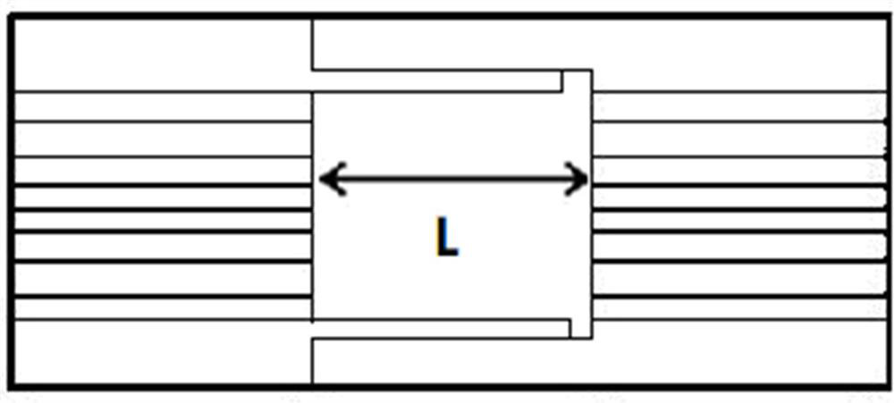
[0005] Recently, a fixed structure of double-array multilayer film waveguide structure has been proposed. By etching a gap with a fixed distance on the multilayer film waveguide structure, two fixed waveguide structures are formed before and after the gap. The gap distance is the first waveguide The length of the primary or secondary focal length of the structure, that is, the second waveguide structure is set at the primary or secondary focus position of the first waveguide structure. The design idea is that after determining the energy of the X-ray, according to the X The calculation method of ray propagation in a single channel (C. Fuhse, T. Salditt, Physica B, 357 (2005) 57-60), by solving the Helmholtz equation of X-rays at the waveguide entrance, the propagation constant (propagation constant ) β and the thickness d of the conducting layer (guiding layer), and then use the Taylor formula to expand the relationship between the small amount of thickness and the small amount of propagation constant, and thus determine the thickness of each conducting layer, according to After the length of the first waveguide structure needs to be preset, use the Fraunhofer diffraction effect equation to determine the focus positions at all levels. After the above calculations, use DC magnetron sputtering technology to prepare multilayer film samples, and then use ion etching ( Reactive Ion Etching) etch the distance of the primary or secondary focal length on the multilayer film sample. This structure can effectively improve the focal signal-to-noise ratio and focus the X-rays in the near field. However, it is found in actual manufacturing that using The thickness of the conduction layer of the multilayer film sample prepared by DC magnetron sputtering technology is often different from the expected thickness, and the fixed gap etched out is often unable to be accurately positioned on the focal distance, and the tiny nanoscale optical elements Errors often cause the focusing effect to be very different from the expected effect, resulting in unsatisfactory focusing effect of the finished product

Method used


Image

  • A Tunable Waveguide System for Nanoscale Focusing of X-rays
  • A Tunable Waveguide System for Nanoscale Focusing of X-rays

Examples


Embodiment Construction

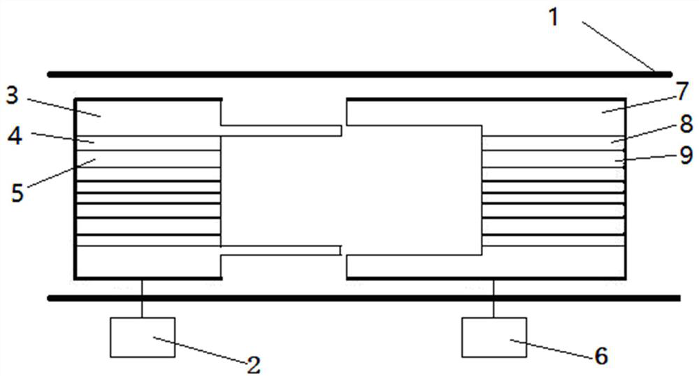
[0022]The present invention will be further described below in conjunction with the accompanying drawings. As the background technology belongs, the principle of the structure and method of the multilayer film waveguide itself is very clear to those skilled in the art. The specific implementation methods of this application only focus on the prior art In addition, it should be noted that the structures in the drawings of the description are only schematic in nature, for example, the number of film layers in the figure is not the real number of layers, as mentioned in the background technology, the number of film layers is actually generally The base number, the middle layer is the conduction layer, and the two sides are the spacer layer, the conduction layer, the spacer layer, etc., and so on. At present, 3-15 layers are mentioned in the prior art. In the embodiment, the waveguide structure of 15 layers is used. To illustrate, in fact, no matter how many layers of the waveguide...


PUM


Abstract

The invention relates to the technology of ionizing radiation processing, especially relates to an X-ray focusing device applying diffraction, refraction or reflection, and particularly relates to anadjustable waveguide system for X-ray nanoscale focusing. The waveguide system comprises a relatively movable adjustable shell base composed of a first shell base and a second shell base. A multilayerthin film waveguide structure with the same structure is fixed in both the first shell base and the second shell base. The whole adjustable shell base is arranged in a temperature adjustable cavity.Compared with the systems in the prior art, two waveguide structures can be applied to adjust and focus the X-rays so that the problems that the expected focusing effect cannot be achieved due to thedifference of the determined parameters in analog computation because of the error in the manufacturing process which cannot be overcome after production and formation of the conventional focusing device can be overcome, and a new way of further improving the X-ray waveguide focusing performance can be provided.

Description

technical field [0001] The present invention relates to a particle or ionizing radiation processing device, such as the field of focusing or moderation, especially to an X-ray focusing device using diffraction, refraction or reflection, specifically an adjustable waveguide system for nanoscale focusing of X-rays and its preparation method. Background technique [0002] The performance and interconnection of nanoscale biological structures are the focus of research in the field of life sciences. In the field of life sciences, the functions and cluster effects of biological molecules have made great progress, but the three-dimensional structure of nanoscale biological structures However, the development of imaging is slow, the main reason is the limitation of three-dimensional imaging technology. Nowadays, the analysis methods used for nanoscale structure imaging mainly include scanning electron microscope analysis, transmission electron microscope analysis and fluorescence a...

Claims


Application Information

Patent Timeline
Patent Type & Authority Patents(China)
IPC IPC(8): G21K1/06
CPCG21K1/06G21K1/062
Inventor 王维维
Owner 深圳市柯尼达医疗设备有限公司
Learn More