A multi-station stage for research and development of PCB boards

A PCB board and multi-station technology, applied in the direction of circuit board tool positioning, electrical components, printed circuit manufacturing, etc., can solve the problems of inability to switch, long moving distance, etc., and achieve the effect of convenient and fast loading and convenient comparison

Active Publication Date: 2019-01-22
ANHUI SHENZE ELECTRONICS TECH
View PDF4 Cites 1 Cited by
  • Summary
  • Abstract
  • Description
  • Claims
  • Application Information

AI Technical Summary

Problems solved by technology

During the R&D process of the PCB board, because the operator needs to place the PCB board on the stage, observe and compare different samples, and find the following shortcomings: 1. The stage can only store one sample at a time, and cannot carry out Switching; 2. The operator needs a long moving distance to place the PCB board on the stage

Method used


Image

  • A multi-station stage for research and development of PCB boards
  • A multi-station stage for research and development of PCB boards
  • A multi-station stage for research and development of PCB boards

Examples


Embodiment Construction

[0019] Through the description of the embodiments below, the specific implementation of the present invention includes the shape, structure, mutual position and connection relationship between the various parts, the function and working principle of each part, the manufacturing process and the operation and use method of the various components involved. etc., to make further detailed descriptions to help those skilled in the art have a more complete, accurate and in-depth understanding of the inventive concepts and technical solutions of the present invention.

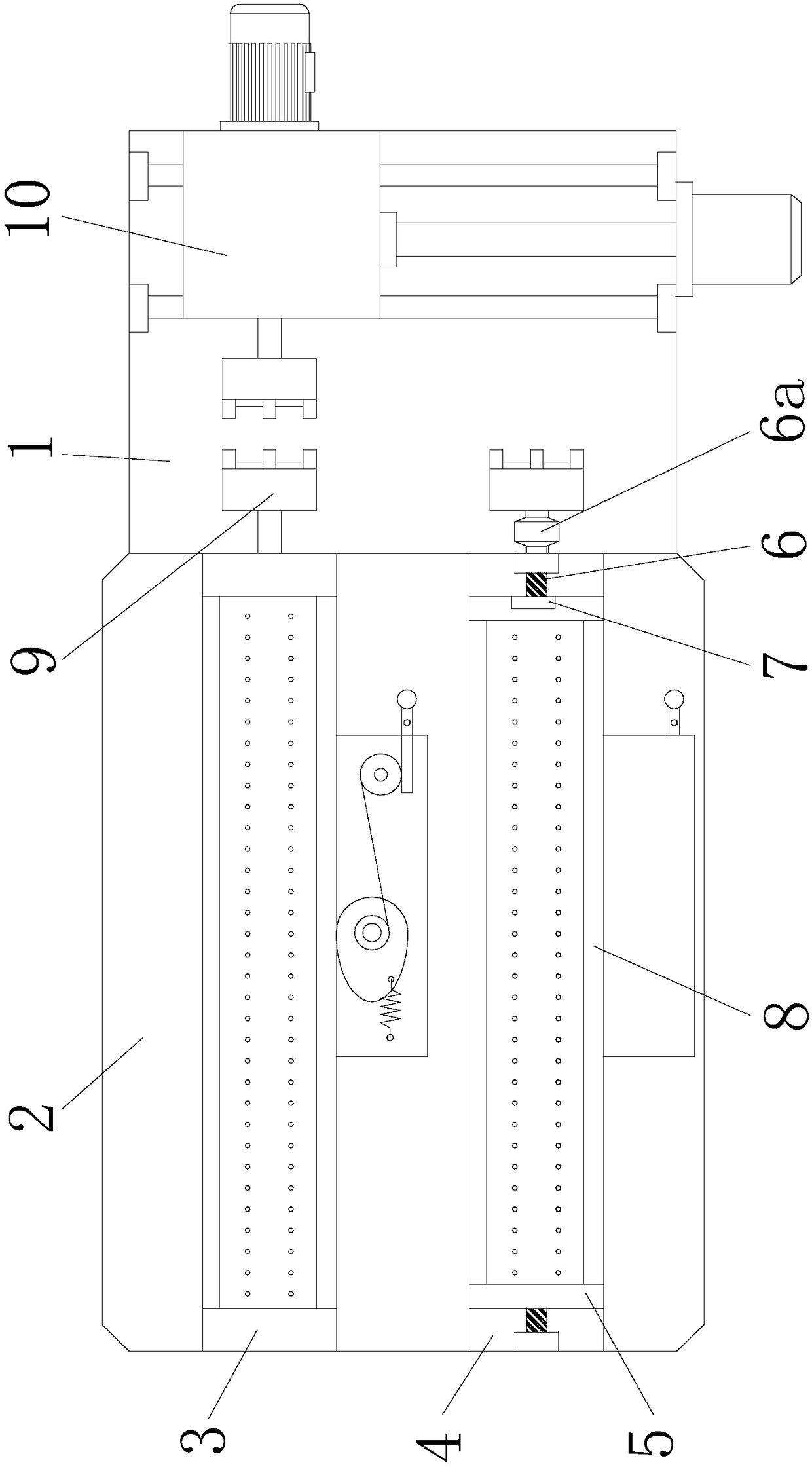
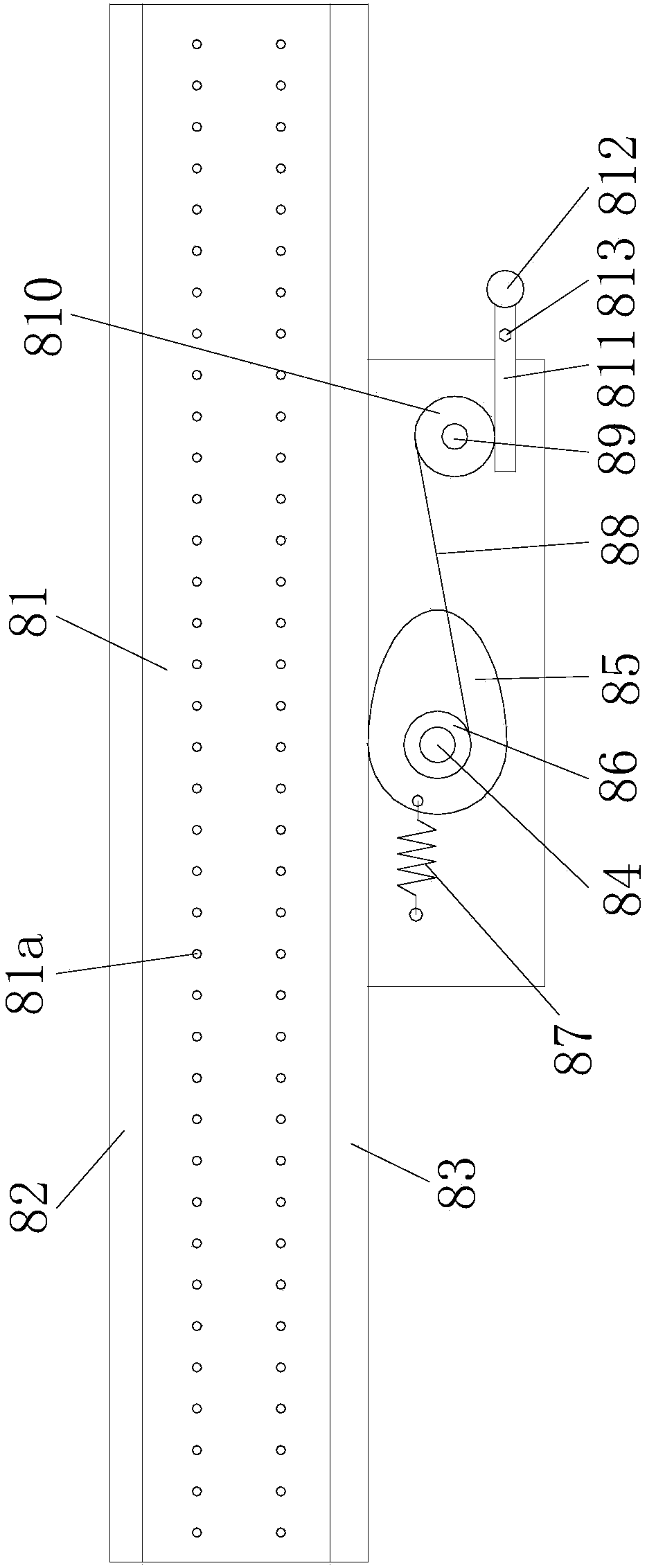
[0020] A multi-station stage for PCB board research and development, including a base 1, a table body 2 is installed on the left part of the base 1, a first station and a second station are arranged on the table body 2, and the first station Including the lower end plate 1 3, the second station includes the lower end plate 2 4, the front part of the upper end surface of the table body 2 is provided with a sliding groove...


PUM


Abstract

The invention provides a multi-station stage for research and development of PCB boards, comprising a base, a stage body is installed on the left part of the base body, a first station and a second station are arranged on the stage body, driven assemblies are installed on the front and rear parts of the base body, a driving assembly is installed on the right part of the base body, and the drivingassembly can provide power for the driven component. The invention adopts the double-station design, which is convenient for operators to quickly carry out comparison and fast feeding of PCB boards, and is provided with a knob and a screw rod for fine adjustment of the second station, so that the PCB boards of the first station and the second station are in relative positions, and the operators are convenient to carry out comparison and fast feeding of PCB boards.

Description

technical field [0001] The invention belongs to the technical field of circuit board production, and in particular relates to a multi-station stage for PCB board research and development. Background technique [0002] With the development of the times, the PCB board manufacturing industry has achieved unprecedented development, and its degree of specialization is getting higher and higher. During the R&D process of the PCB board, because the operator needs to place the PCB board on the stage, observe and compare different samples, and find the following shortcomings: 1. The stage can only store one sample at a time, and cannot carry out Switching; 2. The operator needs a long moving distance to place the PCB board on the stage. Contents of the invention [0003] The purpose of the present invention is to provide a multi-station stage for PCB board research and development, which is dedicated to solving all or one of the problems in the background technology. [0004] In ...

Claims


Application Information

Patent Timeline
Patent Type & Authority Applications(China)
IPC IPC(8): H05K3/00
CPCH05K3/0008
Inventor 赵守江张雷张琳姜广彪胡洪波
Owner ANHUI SHENZE ELECTRONICS TECH
Why Eureka
Try Eureka