Low-energy scanning electron microscope system, scanning electron microscope system and sample detection method

An electron microscope, sample technology, applied in circuits, discharge tubes, measuring devices, etc., to achieve the effect of improving resolution

Active Publication Date: 2019-02-01
FOCUS E BEAM TECH BEIJING CO LTD
View PDF13 Cites 20 Cited by
  • Summary
  • Abstract
  • Description
  • Claims
  • Application Information

AI Technical Summary

Problems solved by technology

[0005] At present, under the condition of low landing point energy, there is no such thing as high resolution, 100% or close to 100% signal electron collection efficiency, flexible detection of backscattered electrons at different emission angles, and flexible control of received signal electrons. Scanning Electron Microscopes of Classes and Other Requirements

Method used


Image

  • Low-energy scanning electron microscope system, scanning electron microscope system and sample detection method
  • Low-energy scanning electron microscope system, scanning electron microscope system and sample detection method
  • Low-energy scanning electron microscope system, scanning electron microscope system and sample detection method

Examples


Embodiment 1

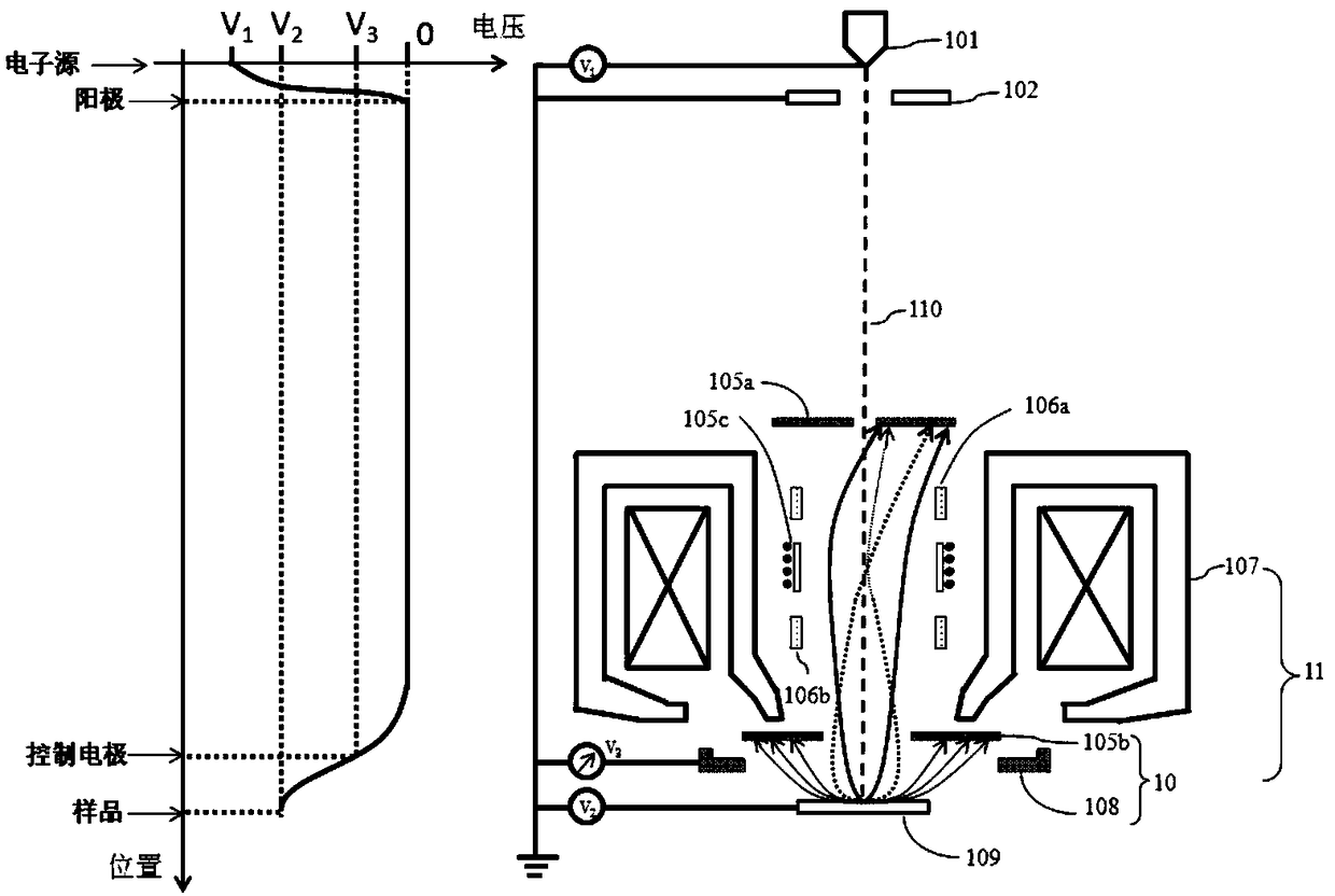
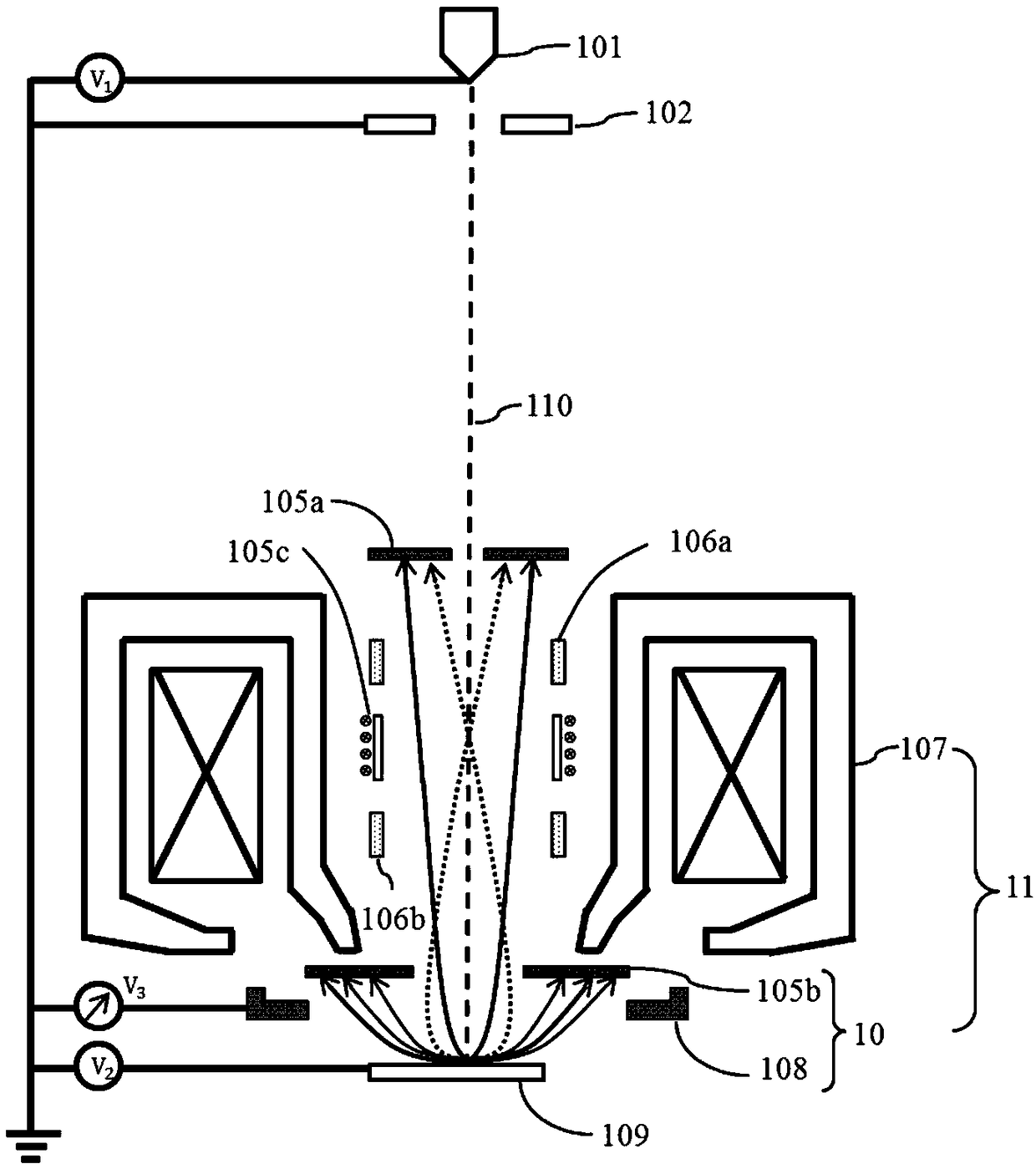
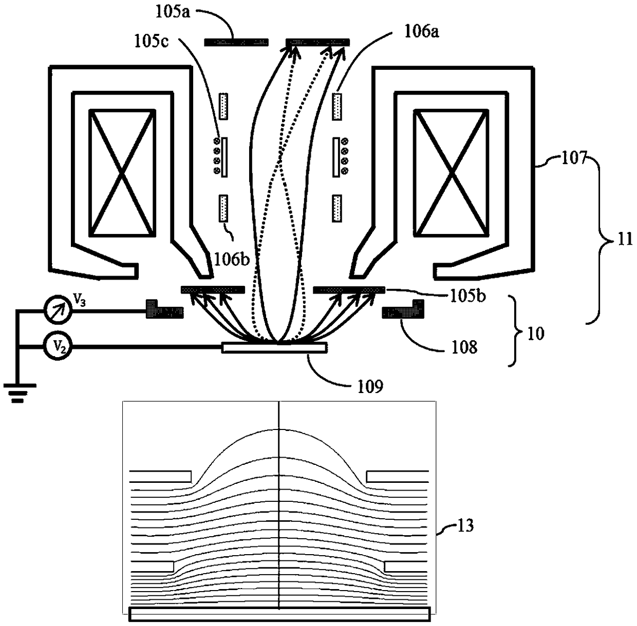
[0114] In view of the above problems, Embodiment 1 of the present invention provides a low-energy scanning electron microscope system, and the composition structure of the scanning electron microscope system is as follows: figure 1 As shown, it includes: a first electron source 101, an electron accelerating structure, a composite objective lens 11 composed of a magnetic lens 107 and an electric lens 10, a first deflection device 106, and a first detection device 105; wherein, the first electron source 101, for generating an electron beam; in an optional embodiment, the first electron source is a first electron source of field emission, such as a first electron source of thermal field emission, or a first electron source of cold field emission , compared with the thermal emission source made of tungsten wire and lanthanum hexaboride material, it has better current density and brightness, and has a smaller virtual source, which can reduce the size of the beam spot generated by th...

Embodiment 2

[0147] The low-energy scanning electron microscope system provided by the second embodiment of the present invention is similar to the scanning electron microscope system provided by the first embodiment of the present invention, the difference is that the composition structure of the scanning electron microscope system provided by the second embodiment of the present invention also includes The electron beam adjustment device is arranged below the anode 102 along the optical axis 110, and is used to change the characteristics of the electron beam after passing through the anode 102; the characteristics of the electron beam at least include: the beam current density of the electron beam and the diameter of the electron beam .

[0148] In an alternative embodiment, such as Figure 4 As shown, the electron beam adjustment device is a converging device 103, which is arranged below the anode 102 along the exit direction of the initial electron beam, and is used to converge the ele...

Embodiment 3

[0151] The low-energy scanning electron microscope system provided in Embodiment 3 of the present invention is similar to the low-energy scanning electron microscope systems provided in Embodiment 1 and Embodiment 2 of the present invention. The difference is that the composition and structure of the low-energy scanning electron microscope system provided by Embodiment 3 of the present invention, such as Figure 5aAs shown, compared with the low-energy scanning electron microscope system provided in Embodiment 1 of the present invention, the electron beam adjustment device is a diaphragm 104, and the diaphragm 104 is located below the anode along the optical axis direction, and is used for scanning the electron beam passing through the anode 102 The electron beam is filtered.

[0152] Or the composition structure of the low-energy scanning electron microscope system provided by Embodiment 3 of the present invention, such as Figure 5b As shown, compared with the low-energy sc...


PUM

PropertyMeasurementUnit
diameteraaaaaaaaaa

Abstract

The present invention discloses a low-energy scanning electron microscope system. The low-energy scanning electron microscope system comprises an electronic source configured to generate an electron beam; an electronic acceleration structure configured to add the motion speed of the electron beam; a compound objective lens configured to perform collection of electronic beams accelerated through the electronic acceleration structure; a deflection device configured to change the movement direction of the electronic beams; a detection device comprising a first sub detection device configured to receive secondary electrons and backscattered electrons generated on the samples, a second sub detection device configured to receive the backscattered electrons and a control device configured to change the movement directions of the secondary electrons and the backscattered electrons; and an electric lens comprising the second sub detection device, a sample table and a control electrode and configured to reduce the movement speed of the electronic beams and change the movement directions of the secondary electrons and the backscattered electrons. The present invention further discloses a scanning electron microscope system and a sample detection method.

Description

technical field [0001] The invention relates to scanning electron microscope technology, in particular to a low-energy scanning electron microscope system, a scanning electron microscope system and a sample detection method. Background technique [0002] Scanning electron microscopes are widely used to observe the characteristics of samples in the micron or nanometer size range; when observing non-metallic samples such as biological samples or semiconductor samples, scanning electron microscopes with low drop point energy (energy less than 3keV) can reduce damage to samples and charge effect and widely used. [0003] On the one hand, under the condition of low drop point energy, most of the samples to be detected are non-conductive materials. In order to prevent the charging effect or damage the samples, the incident scanning electron beam current is usually very small, only a few hundred pA or even several pA, so the excitation from the sample There are very few signal ele...

Claims


Application Information

Patent Timeline
Patent Type & Authority Applications(China)
IPC IPC(8): H01J37/145H01J37/244H01J37/26H01J37/28G01N23/203G01N23/225
CPCH01J37/12H01J37/141H01J37/145H01J37/1474H01J37/244H01J37/263H01J37/265H01J37/28G01N23/203G01N23/2251G01N2223/418H01J2237/2804H01J2237/2806H01J2237/04756H01J2237/121H01J2237/103H01J2237/2449H01J37/1475H01J37/1477H01J2237/0473H01J2237/1516H01J2237/24475H01J2237/2448H01J2237/24495H01J2237/2446
Inventor 李帅何伟
Owner FOCUS E BEAM TECH BEIJING CO LTD
Why Eureka
Try Eureka