A Silicon Wafer Primary Negative Pressure Diffusion Process
A diffusion process and silicon wafer technology, which is applied in the manufacture of electrical components, circuits, semiconductors/solid-state devices, etc., can solve the problems of cumbersome process manufacturing, diffusion of volatile phosphorus sources, and low diffusion efficiency, so as to improve diffusion efficiency and reduce back-to-source , The effect of simplifying the coating process
- Summary
- Abstract
- Description
- Claims
- Application Information
AI Technical Summary
Problems solved by technology
Method used
Image

Examples
Embodiment Construction
[0025] The present invention will be further described below in conjunction with the accompanying drawings and specific embodiments.
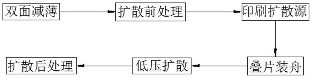
[0026] Such as figure 1 As shown, the present invention relates to a silicon chip negative pressure diffusion process, comprising the following steps:
[0027] 1) Double-sided thinning of the silicon wafer: use an etching solution to etch the silicon wafer on both sides to remove the surface damage layer, specifically including the following steps:
[0028] A. Use a thermometer to measure the temperature of the etching solution. The temperature is generally 0-15°C, and set the etching time of the silicon wafer according to the temperature of the etching solution. The etching time is generally 9-50s. Determine the etching time according to the temperature of the etching solution. Place in the etching solution for etching and thinning, and determine the thickness of the single-sided thinning of the silicon wafer according to the temperature of t...
PUM
 Abstract
Description
Claims
Application Information