Focusing method in wafer detection process and wafer detection device

A focusing method and detection device technology, applied in semiconductor/solid-state device testing/measurement, electrical components, semiconductor/solid-state device manufacturing, etc., can solve problems such as low accuracy of detection results, avoid inaccurate focusing and improve accuracy and reliability effects

Inactive Publication Date: 2019-03-01
HUAIAN IMAGING DEVICE MFGR CORP
View PDF3 Cites 4 Cited by
  • Summary
  • Abstract
  • Description
  • Claims
  • Application Information

AI Technical Summary

Problems solved by technology

[0006] The invention provides a focusing method and a wafer detection device in the wafer detection process, which are used to solve the problem of

Method used


Image

  • Focusing method in wafer detection process and wafer detection device
  • Focusing method in wafer detection process and wafer detection device
  • Focusing method in wafer detection process and wafer detection device

Examples


Example Embodiment

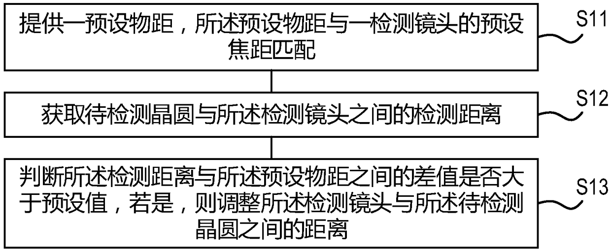
[0044] Specific implementations of the focusing method and wafer inspection device in the wafer inspection process provided by the present invention will be described in detail below in conjunction with the accompanying drawings.

[0045] This embodiment provides a focusing method in the wafer inspection process, with figure 1 It is a flowchart of the focusing method in the wafer inspection process in the specific embodiment of the present invention. Such as figure 1 As shown, the focusing method in the wafer inspection process provided in this embodiment includes the following steps:

[0046] In step S11, a preset object distance is provided, and the preset object distance matches a preset focal length of a detection lens.

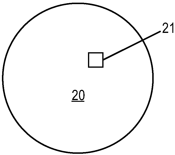
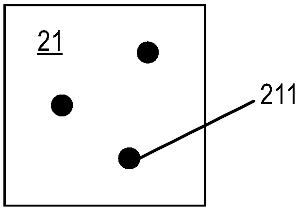
[0047] Attached Figure 2A-2B It is a schematic diagram of the structure of the reference wafer in the specific embodiment of the present invention. image 3 It is a schematic diagram of the structure of the reference wafer and the inspection lens in the specifi...


PUM


Abstract

The invention relates to the technical field of semiconductor manufacturing, in particular to a focusing method in a wafer detection process and a wafer detection device. The focusing method in the wafer detection process comprises the steps of providing a preset object distance, wherein the preset object distance is matched with a preset focus of a detection lens; acquiring a detection distance between a to-be-detected wafer and the detection lens; and judging whether difference between the detection distance and the preset object distance is larger than a preset value, if yes, adjusting thedistance between the detection lens and the to-be-detected wafer. By the focusing method, the problem of focusing inaccuracy of a detection machine table caused by different wafer heights is prevented, and the accuracy and the reliability of a wafer detection result are improved.

Description

technical field [0001] The invention relates to the technical field of semiconductor manufacturing, in particular to a focusing method in a wafer inspection process and a wafer inspection device. Background technique [0002] With the development of mobile terminals such as smart phones and tablet computers in the direction of miniaturization, intelligence, and energy saving, the high performance and integration of chips are becoming more and more obvious, which prompts chip manufacturers to actively adopt advanced technology to manufacture faster and more economical products. The pursuit of electric chips intensified. In particular, the main components of many wireless communication devices require advanced semiconductor technologies and processes below 40nm. Therefore, the demand for advanced process capacity has increased significantly compared with the past, driving integrated circuit manufacturers to continuously improve the level of process technology. In order to imp...

Claims


Application Information

Patent Timeline
IPC IPC(8): H01L21/66H01L21/67H01L21/68
CPCH01L21/67253H01L21/67259H01L21/681H01L22/12H01L22/20
Inventor 于洋黄仁德方桂芹
Owner HUAIAN IMAGING DEVICE MFGR CORP
Why Eureka
Try Eureka