Non-volatile memory with restricted dimensions

A memory, memory word technology, applied in the field of memory, can solve the problem that the separation voltage solution is not suitable, etc.

Active Publication Date: 2019-03-05
STMICROELECTRONICS (ROUSSET) SAS
View PDF5 Cites 0 Cited by
  • Summary
  • Abstract
  • Description
  • Claims
  • Application Information

AI Technical Summary

Problems solved by technology

[0018] However, it is desirable to limit the use of the surface area of ​​the semiconductor substrate supporting the integrated circuit, so a split voltage solution may not be suitable, for example for applications including already small Low-density memory of the memory plane, which therefore cannot accept large surface areas at the periphery

Method used


Image

  • Non-volatile memory with restricted dimensions
  • Non-volatile memory with restricted dimensions
  • Non-volatile memory with restricted dimensions

Examples


Embodiment Construction

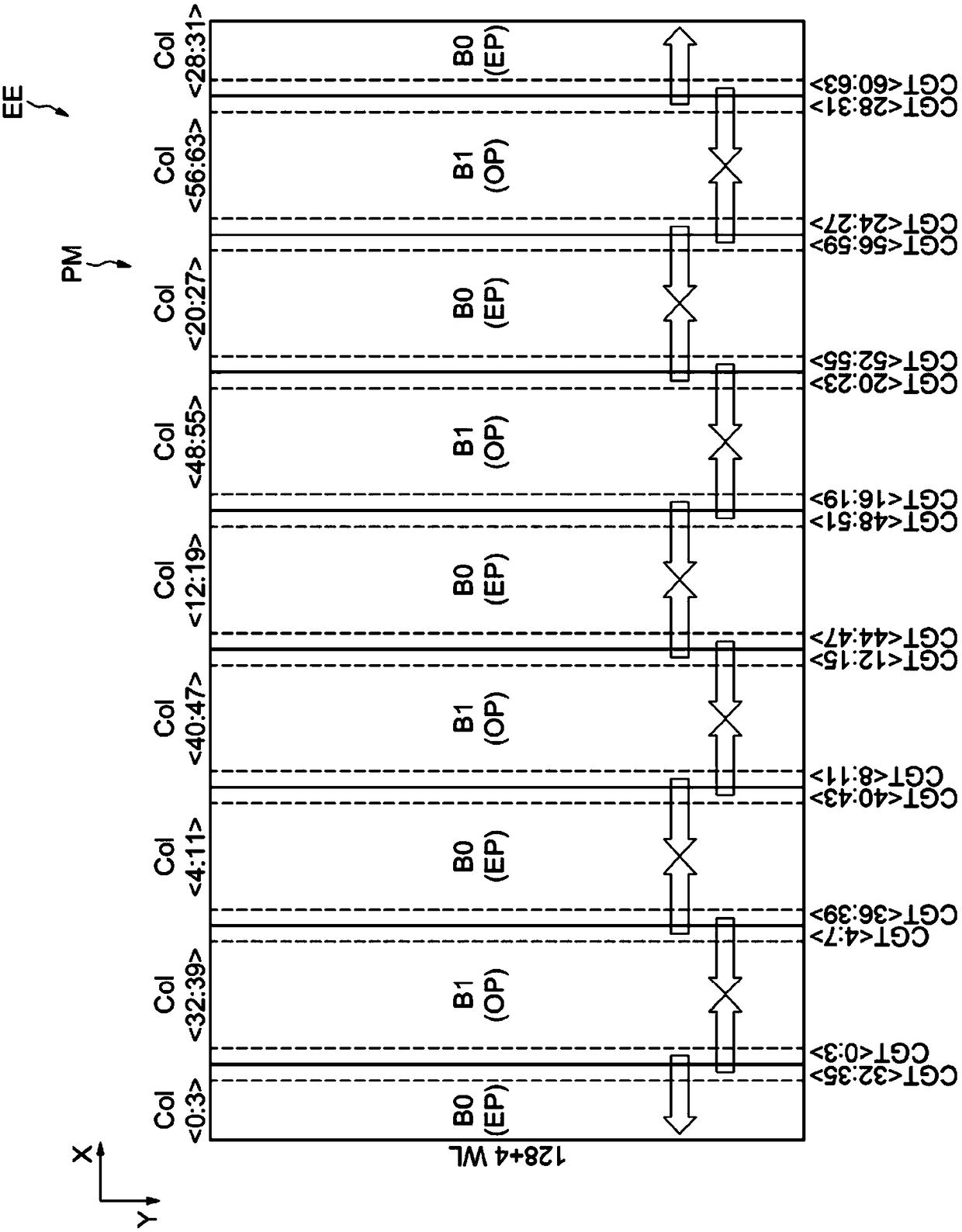
[0029] A solution is proposed that makes it possible to address the voltage limitations of the components while reducing the surface area consumed both in the memory plane and at the periphery.

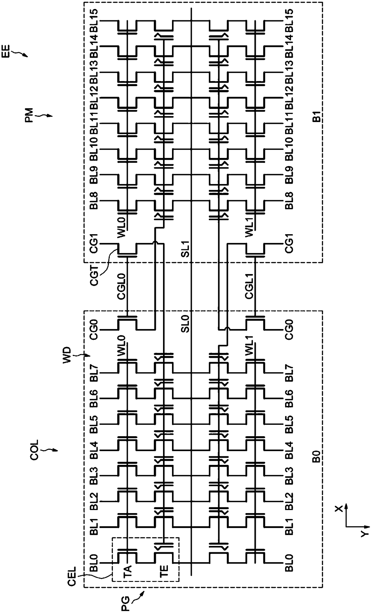
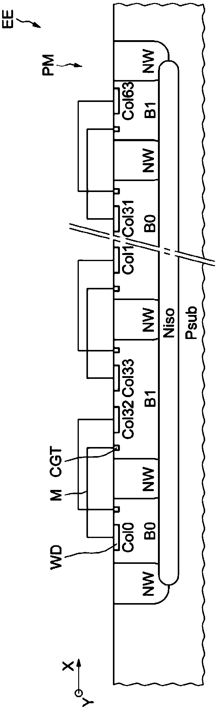
[0030] In this respect it is therefore proposed a memory device of the electrically erasable programmable non-volatile memory type comprising a memory plane comprising a series of adjacent semiconductor grooves of a first conductivity type electrically insulated from each other, each each memory cell includes a state transistor having a floating gate and a control gate, each control gate The select transistors are coupled to the control gates of the state transistors of the memory word to which it is assigned, each control gate select transistor being located in and on an adjacent semiconductor recess housing the semiconductor recess of the memory word to which it is assigned.

[0031] Thus, it is possible to increase the potential of the groove comprising the control gate selection t...


PUM

PropertyMeasurementUnit
thicknessaaaaaaaaaa

Abstract

The invention relates to a non-volatile memory with restricted dimensions. A memory device includes a memory plane including a succession of neighboring semiconductor recesses of a first type of conductivity, wherein each semiconductor recess houses a plurality of memory words including a plurality of memory cells, wherein each memory cell includes a state transistor having a floating gate and a control gate. The memory device further includes a plurality of control gate selection transistors respectively allocated to each memory word of the plurality of memory words, wherein each control gateselection transistor is coupled to the control gates of the state transistors of the memory word to which the control gate selection transistor is allocated, wherein each control gate selection transistor is situated in and on a neighbor semiconductor recess of the semiconductor recess housing the memory word to which the control gate selection transistor is allocated.

Description

[0001] Cross References to Related Applications [0002] This application claims priority from French Patent Application No. 1757908 filed on August 28, 2017, which is hereby incorporated by reference. technical field [0003] Embodiments relate to memory, particularly non-volatile memory, and in certain embodiments to non-volatile memory having constrained (eg, compact) size. Background technique [0004] Typically in an EEPROM memory device, a memory cell comprises a state transistor intended to store an item of information. The state transistor includes a control gate and a floating gate in series with an access transistor or a bit line select transistor. The access transistor is controlled by the word line signal and makes it possible to electrically access the state transistor, in particular in order to read a data item from it or write a data item to it. [0005] The control gate select transistor is connected between the gate control line and the control gate of th...

Claims


Application Information

Patent Timeline
Patent Type & Authority Applications(China)
IPC IPC(8): G11C16/02
CPCG11C16/02G11C5/025G11C16/0433G11C16/06H10B41/41H10B41/35H10B41/40G11C16/10G11C16/14
Inventor F·塔耶特M·巴蒂斯塔
Owner STMICROELECTRONICS (ROUSSET) SAS
Why Eureka
Try Eureka