
Eureka
For R&D, Eureka makes reading and utilizing patents & technical documents easy.
Eureka AIR
Designed for self-driven R&D workflows. Generate viable solutions, solve complex R&D challenges, empower your innovation with AI.

Eureka Materials
Designed for material experts only. Revolutionize your material R&D, from search, analyze, to developing new materials.

TechResearch
Generate reliable direction feasibility study reports for your R&D in just a few steps.

TechSeek
Discover and master advanced knowledge NOW. Basics, ideas, possibilities, all at once.

TechMind
As an expert in R&D Theories, TechMind can generates customized viable solutions instantly.

TechRisk
Analyze your overall solution with one click, know your potential R&D risks in advance.

TechMonitor
Get weekly tech updates, stay abreast of the latest tech innovations and key insights.
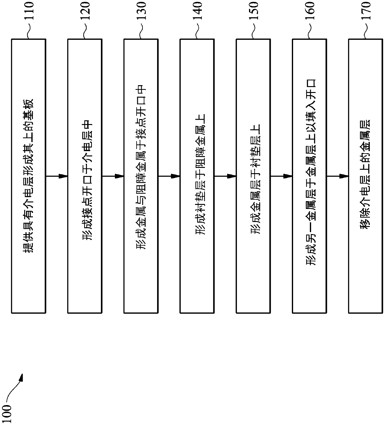
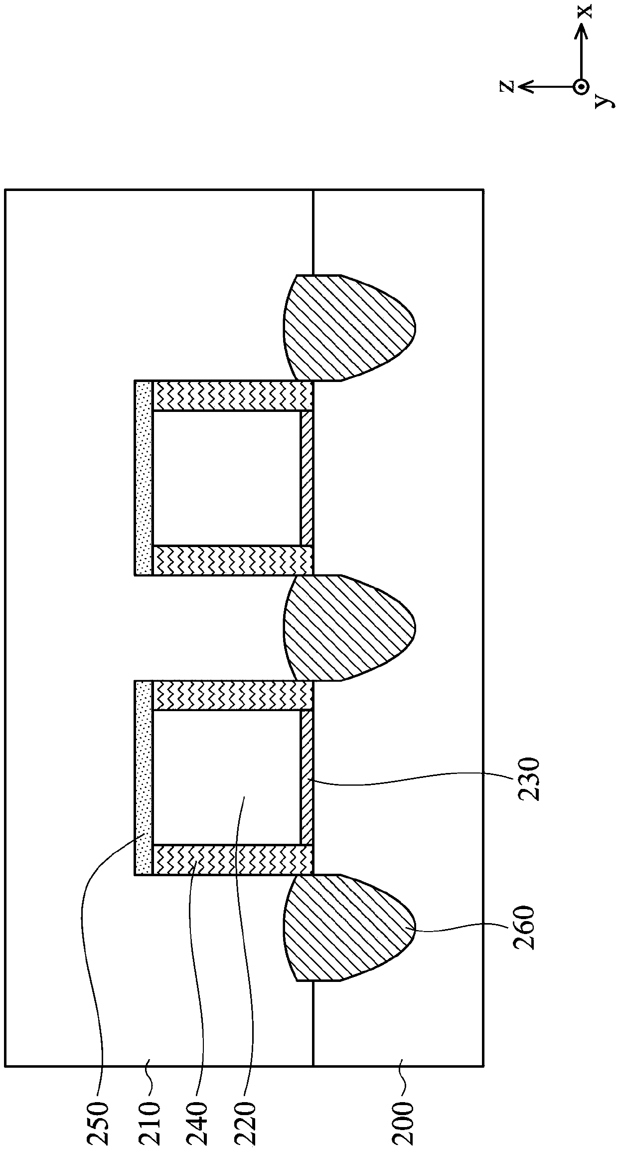
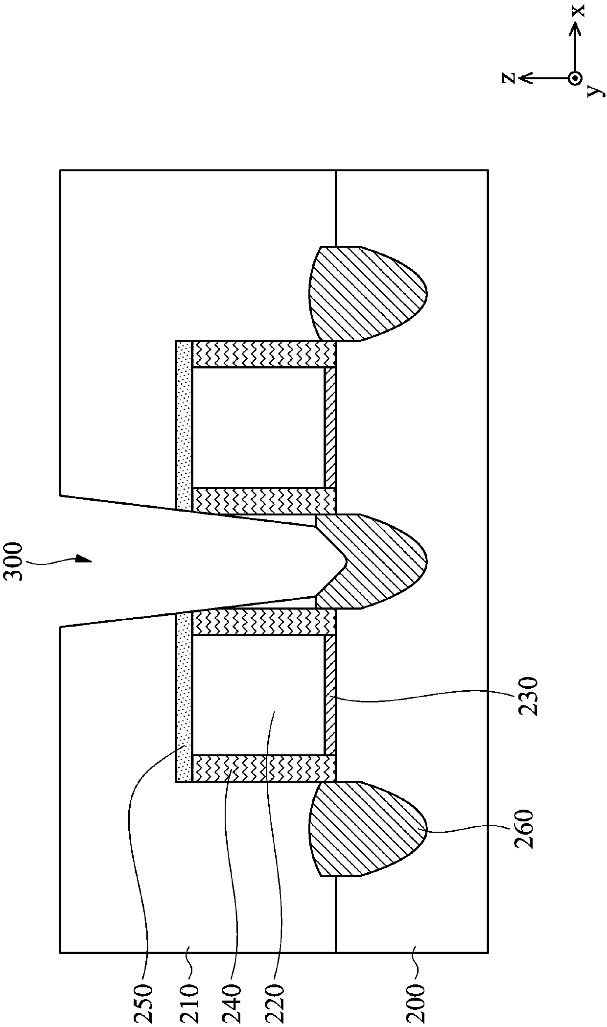
Forming method of semiconductor structure
A semiconductor and contact technology, applied in the field of metallization process, can solve the problems of affecting the reliability of integrated circuits and increasing contact resistance.
- Summary
- Abstract
- Description
- Claims
- Application Information
AI Technical Summary
Problems solved by technology
Method used
Image

Examples
Embodiment Construction
[0041] It is to be understood that different embodiments or examples provided below may implement different configurations of the present invention. The examples of specific components and arrangements are used to simplify the invention and not to limit the invention. For example, the statement that the first component is formed on the second component includes that the two are in direct contact, or there are other additional components interposed between the two instead of direct contact. In addition, numbers may be repeated in various examples of the present invention, but these repetitions are only for simplification and clarity of illustration, and do not mean that units with the same numbers in different embodiments and / or arrangements have the same corresponding relationship.
[0042] In addition, spatial relative terms such as "below", "beneath", "lower", "above", "above", or similar terms may be used to simplify describing the relationship between one element and anoth...
PUM
| Property | Measurement | Unit |
|---|---|---|
| thickness | aaaaa | aaaaa |
| thickness | aaaaa | aaaaa |
Abstract
Description
Claims
Application Information
 - R&D Engineer
- R&D Manager
- IP Professional
- Industry Leading Data Capabilities
- Powerful AI technology
- Patent DNA Extraction
Browse by: Latest US Patents, China's latest patents, Technical Efficacy Thesaurus, Application Domain, Technology Topic, Popular Technical Reports.
© 2024 PatSnap. All rights reserved.Legal|Privacy policy|Modern Slavery Act Transparency Statement|Sitemap|About US| Contact US: help@patsnap.com