Pixel structure and display panel

A technology of pixel structure and pixel area, used in character and pattern recognition, instruments, semiconductor devices, etc., can solve problems such as poor recognition of fingerprint sensors

Inactive Publication Date: 2019-05-28
KUNSHAN GO VISIONOX OPTO ELECTRONICS CO LTD
View PDF5 Cites 11 Cited by
  • Summary
  • Abstract
  • Description
  • Claims
  • Application Information

AI Technical Summary

Problems solved by technology

[0003] Based on this, it is necessary to provide a pixel structure and a display pane

Method used


Image

  • Pixel structure and display panel
  • Pixel structure and display panel
  • Pixel structure and display panel

Examples


Embodiment Construction

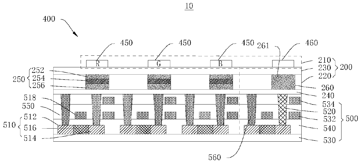
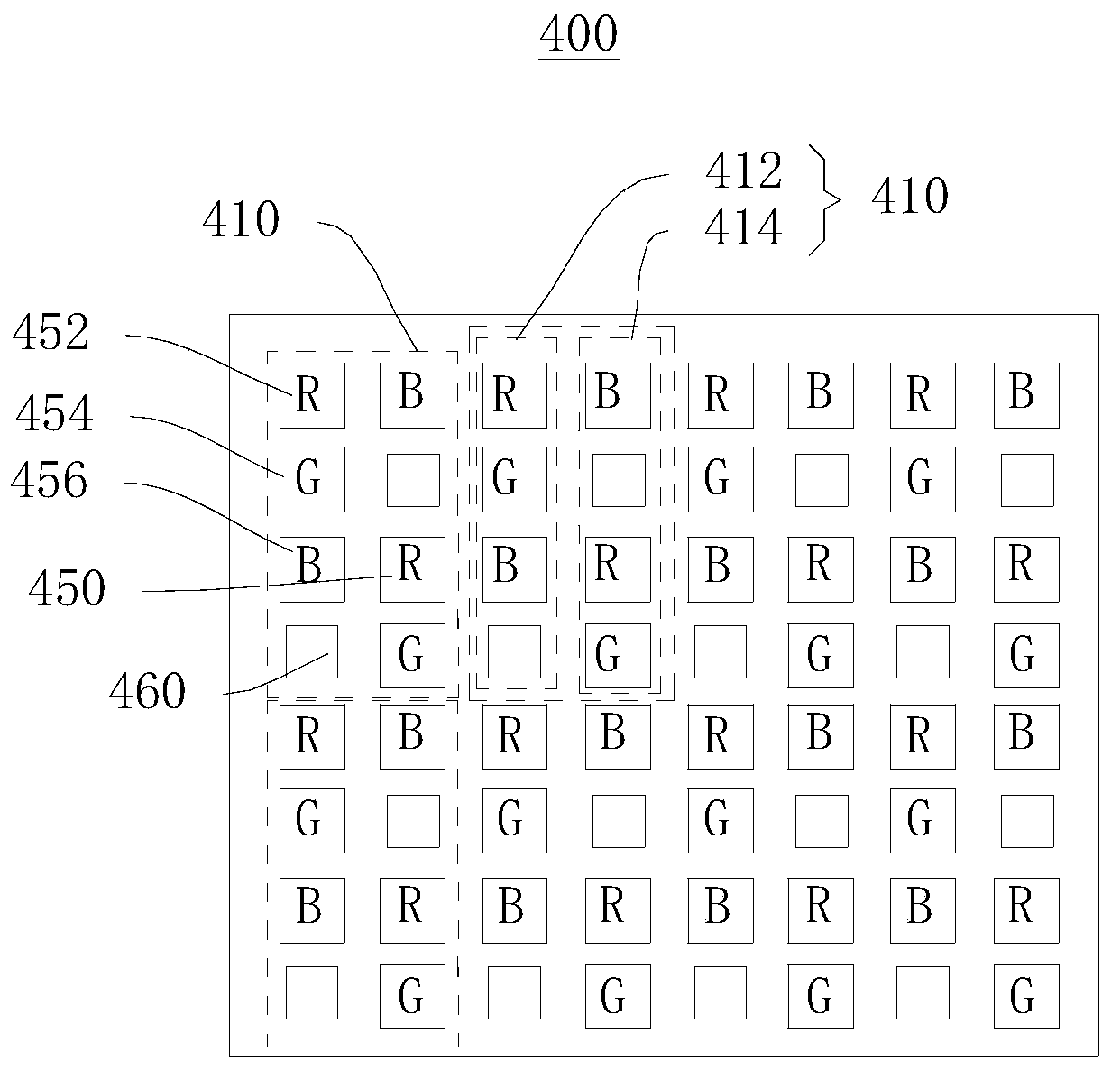
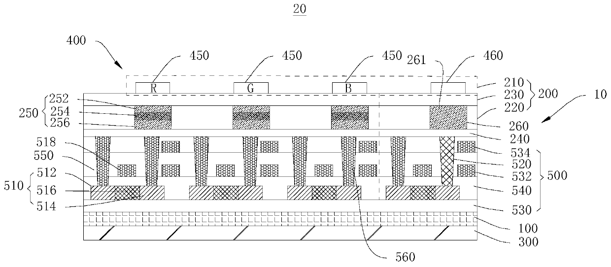
[0065] In order to make the purpose, technical solution and advantages of the present application clearer, the pixel structure and the display panel of the present application will be further described in detail through the following embodiments in conjunction with the accompanying drawings. It should be understood that the specific embodiments described here are only used to explain the present application, not to limit the present application.

[0066] The serial numbers assigned to components in this document, such as "first", "second", etc., are only used to distinguish the described objects, and do not have any sequence or technical meaning. The "connection" and "connection" mentioned in this application all include direct and indirect connection (connection) unless otherwise specified. In the description of this application, it should be understood that the terms "upper", "lower", "front", "rear", "left", "right", "vertical", "horizontal", "top", The orientation or posi...


PUM


Abstract

The invention relates to a pixel structure and a display panel. The pixel structure includes a light emitting functional layer. The light-emitting functional layer comprises a pixel area array. The pixel area array comprises a plurality of light-emitting pixel areas and at least one light-transmitting pixel area. The light-transmitting pixel area can improve the light transmittance of the displaypanel, so that the amount of the fingerprint identification light received by the fingerprint identifier can be increased, the identification precision of the fingerprint identifier is improved, and the imaging efficiency is improved.

Description

technical field [0001] The present application relates to the display field, in particular to a pixel structure and a display panel. Background technique [0002] In the field of display, touch screen technology has developed more and more rapidly, which brings great convenience to people's use. However, in the traditional technology, due to the scattered and small light transmission area of ​​the unit pixel in the screen, the overall light transmittance of the screen is low, which easily leads to poor recognition of the fingerprint sensor under the screen and poor imaging effect. Contents of the invention [0003] Based on this, it is necessary to provide a pixel structure and a display panel to solve the problem of poor recognition of the fingerprint sensor under the screen. [0004] A pixel structure comprising: [0005] The light-emitting functional layer includes a pixel area array, and the pixel area array includes a plurality of light-emitting pixel areas and at l...

Claims


Application Information

Patent Timeline
IPC IPC(8): H01L27/32G06K9/00
Inventor 丁伟陈心全
Owner KUNSHAN GO VISIONOX OPTO ELECTRONICS CO LTD
Why Eureka
Try Eureka