
A microstructure packaging method and a packaging device
A packaging method and microstructure technology, applied in the direction of microstructure devices, manufacturing microstructure devices, microstructure technology, etc., can solve the problems of insufficient filling of microholes/groove edges, slow filling speed of small cavities, complex front and rear processes, etc. , to achieve the effects of reducing the difficulty of filling, reducing the volume of the microstructure, and increasing the reliability
- Summary
- Abstract
- Description
- Claims
- Application Information
AI Technical Summary
Problems solved by technology
Method used
Image

Examples
Embodiment Construction
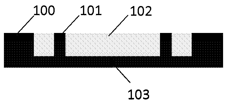
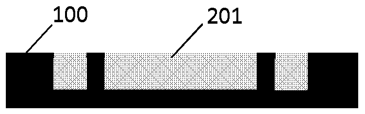
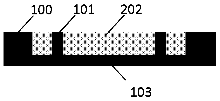
[0048] According to the basic idea of the present disclosure, a microstructure encapsulation method is provided, including: etching conductive silicon pillars and silicon grooves on the upper surface of a single crystal silicon wafer, and remaining between the bottom of the silicon groove and the back surface of the single crystal silicon wafer The monocrystalline silicon material is the microstructure functional layer; the glass powder is filled into the silicon groove; the glass powder is sintered at a temperature above the softening point of the glass powder to form a glass body; the functional structure is etched on the back of the monocrystalline silicon wafer The microstructure and frame of the electrical connection structure; the cap and the frame are bonded by bonding process, the microstructure is hermetically packaged, and metal electrodes are deposited on the conductive silicon pillars to achieve ohmic contact with the external circuit. This method discretizes the ...
PUM
 Abstract
Description
Claims
Application Information