Scan signal line driving circuit and display device including same
A technology for scanning signal lines and driving circuits, which is applied in information storage, static indicators, electrical digital data processing, etc., and can solve problems such as unstable operation, abnormality, and leakage current (increased turn-off leakage current) of the gate driver
- Summary
- Abstract
- Description
- Claims
- Application Information
AI Technical Summary
Problems solved by technology
Method used
Image

Examples
no. 1 approach
[0082]
[0083] Figure 4 It is a block diagram for explaining the schematic structure of the gate driver 200 in this embodiment. The gate driver 200 in this embodiment is disposed on one end side of the display unit 400 ( Figure 4 The shift register 210L on the left side in ) and the other end side of the display unit 400 ( Figure 4 The shift register 210R on the right side of ) is constituted. There are i gate bus lines GL( 1 )˜GL(i) disposed in the display unit 400 , the shift register 210L drives the odd-numbered row gate bus lines GL, and the shift register 210R drives the even-numbered row gate bus lines GL. That is, in the present embodiment, the gate bus lines GL( 1 ) to GL(i) are driven by a driving method called “comb-tooth driving” or “staggered driving”.
[0084] The shift register 210L is composed of p unit circuits 2L( 1 ) to 2L(p), and the shift register 210R is composed of p unit circuits 2R( 1 ) to 2R(p). P is i / 4. It should be noted, Figure 4 In th...
no. 2 approach
[0140]
[0141] Figure 14 It is a block diagram for explaining the schematic structure of the gate driver 200 in this embodiment. Like the first embodiment, the gate driver 200 in this embodiment also includes a shift register 210L disposed at one end of the display unit 400 and a shift register 210R disposed at the other end of the display unit 400 . In this embodiment, the difference from the first embodiment is that each of the gate bus lines GL( 1 ) to GL(i) is driven by both the shift register 210L and the shift register 210R. That is, each of the gate bus lines GL( 1 ) to GL(i) is driven from both the one end side and the other end side.
[0142] The shift register 210L is composed of p unit circuits 2L( 1 ) to 2L(p), and the shift register 210R is composed of p unit circuits 2R( 1 ) to 2R(p). P is i / 2. As in the first embodiment, each unit circuit 2 is connected to two gate bus lines GL.
[0143]
[0144] Figure 15 It is a block diagram showing the configurat...
no. 3 approach
[0161] Figure 19 It is a block diagram for explaining the schematic structure of the gate driver 200 in this embodiment. The gate driver 200 in this embodiment is constituted by a shift register 210 disposed on one end side of the display unit 400 . The shift register 210 is composed of p unit circuits 2(1) to 2(p). P is i / 2. Each unit circuit 2 is connected to two gate bus lines GL.
[0162] Depend on Figure 14 and Figure 19 It can be seen that in the second embodiment, each of the gate bus lines GL(1) to GL(i) is driven from both the one end side and the other end side, but in this embodiment, each gate bus line GL(1) to GL (i) Driven by only one end side. The second embodiment differs from the present embodiment only in this point, and therefore descriptions of the configuration of the shift register, the configuration of the unit circuit, and the operation of the gate driver are omitted.
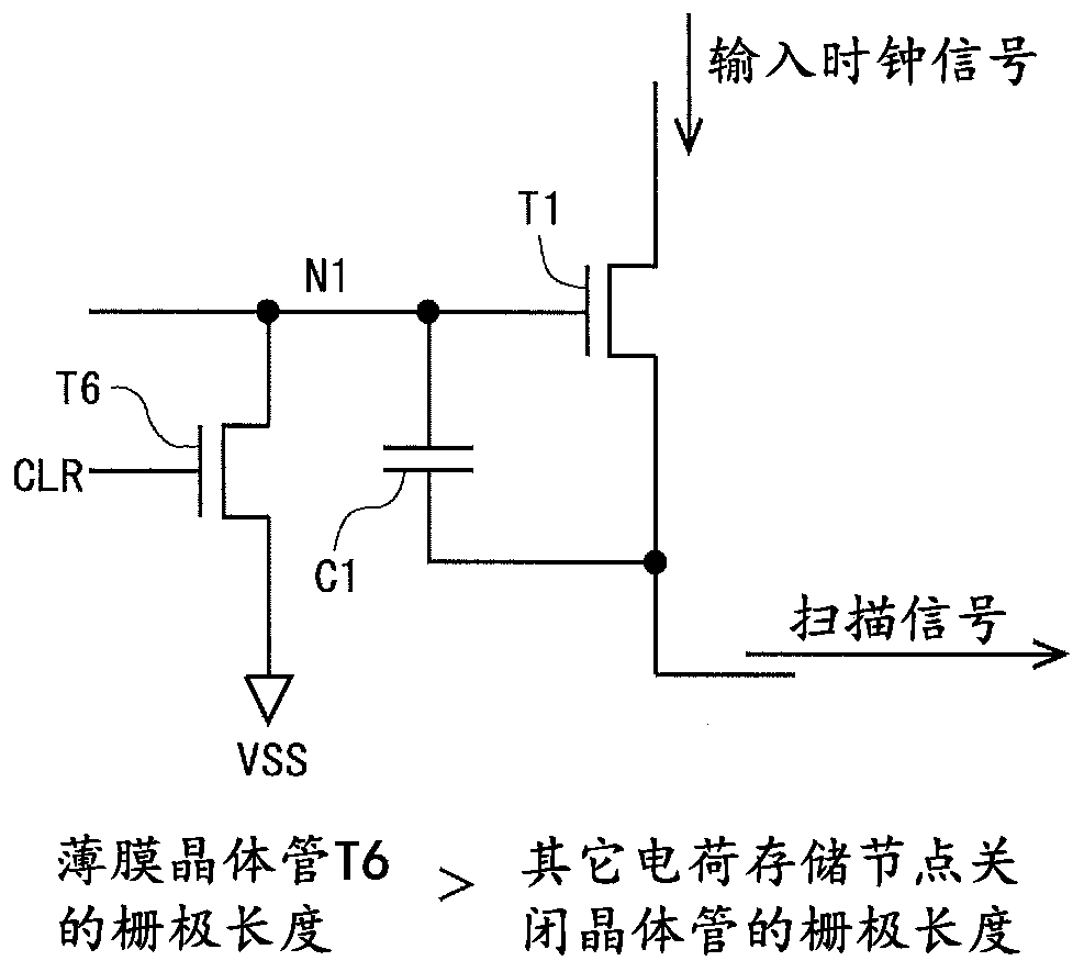
[0163] In addition, regarding measures against charge leakage, in the pres...
PUM
 Abstract
Description
Claims
Application Information