Printed circuit board manufacturing method

A technology for printed circuit boards and manufacturing methods, which is applied in the fields of printed circuit manufacturing, printed circuit, multi-layer circuit manufacturing, etc., can solve problems such as delamination of exploding boards, insufficient filling of glue, etc., to increase the pressing buffer force between layers, Solve the problem of insufficient filling and reduce the effect of delamination

Inactive Publication Date: 2019-07-23
ZHUHAI CHINA EAGLE ELECTRONIC CIRCTCUIS CO LTD +1
View PDF5 Cites 0 Cited by
  • Summary
  • Abstract
  • Description
  • Claims
  • Application Information

AI Technical Summary

Problems solved by technology

[0003] The embodiment of the present invention provides a method for manufacturing a printed circuit board to solve the problems of insufficient glue filling and delamination of the board in the existing method of manufacturing an ultra-thick copper printed circuit board

Method used


Image

  • Printed circuit board manufacturing method
  • Printed circuit board manufacturing method
  • Printed circuit board manufacturing method

Examples


Embodiment Construction

[0023] The following will clearly and completely describe the technical solutions in the embodiments of the present invention with reference to the accompanying drawings in the embodiments of the present invention. Obviously, the described embodiments are some of the embodiments of the present invention, but not all of them. Based on the embodiments of the present invention, all other embodiments obtained by persons of ordinary skill in the art without creative efforts fall within the protection scope of the present invention.

[0024] In order to illustrate the technical solution of the present invention, specific examples are given below.

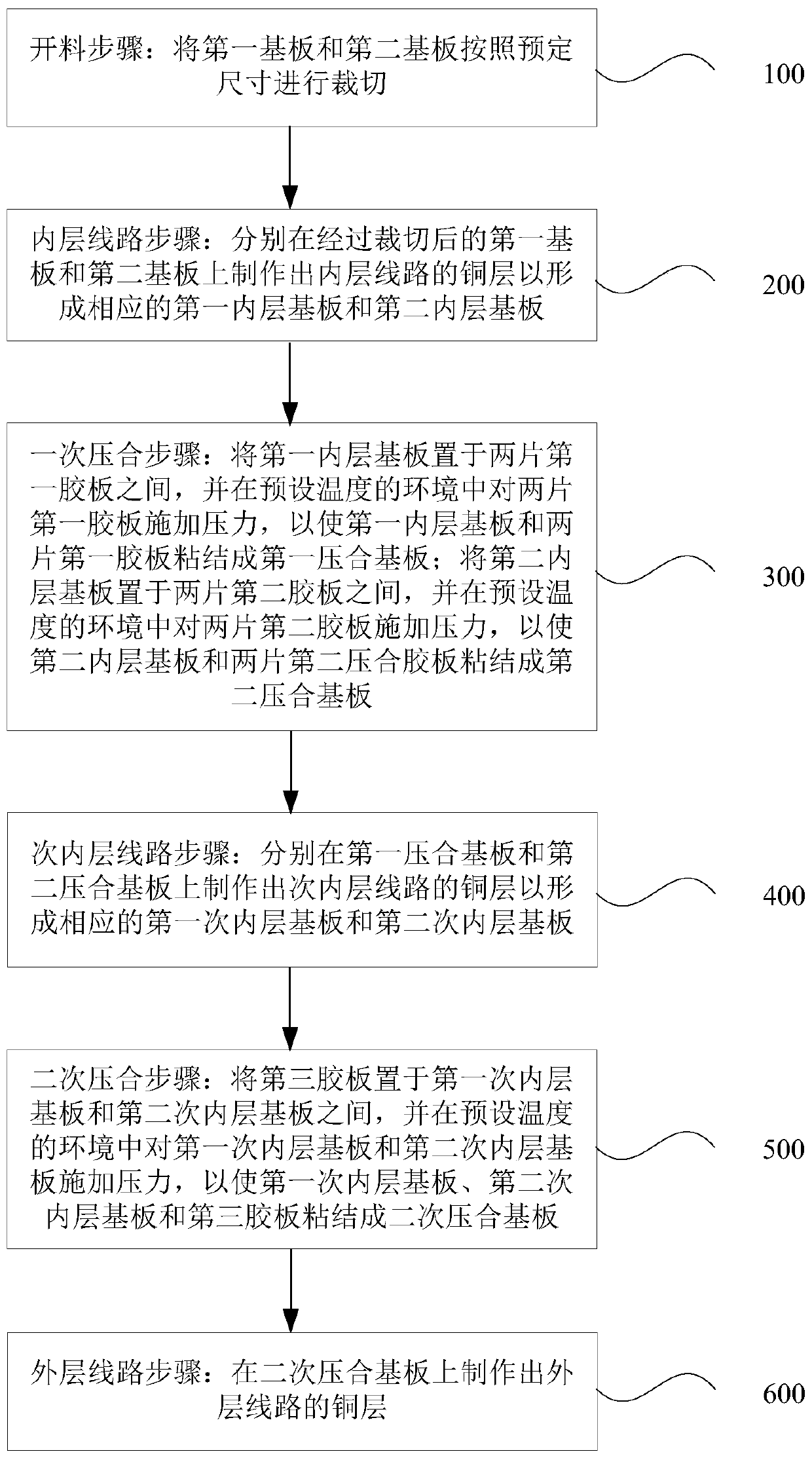
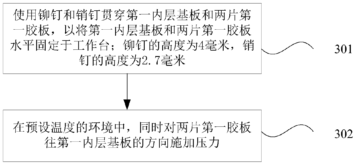
[0025] In this example, if figure 1 Shown, provide a kind of printed circuit board manufacturing method, this method comprises the steps:

[0026] Cutting step 100: cutting the first substrate and the second substrate according to a predetermined size.

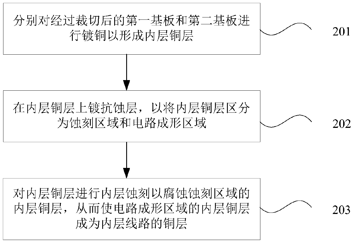
[0027] Inner-layer circuit step 200 : respectively fabricating copper layers of inn...


PUM


Abstract

The invention relates to the field of printed circuit board processing and provides a printed circuit board manufacturing method. The method comprises a cutting step, an inner layer circuit step, a primary pressing step, a secondary inner layer circuit step, a secondary pressing step and an outer layer circuit step, the glass state conversion temperature of a first substrate and a second substrateis higher than 170 DEG C, a first rubber plate and a second rubber plate both comprise three polypropylene plates, and a third rubber plate comprises four polypropylene plates; the thickness of the polypropylene plate is 3.8 mils, the thickness of glass cloth is 2.1 mils, the thickness of resin is 1.6 mils, and the glue content is 71%. Therefore, the requirement that the glue filling amount is very large in the manufacturing process of the ultra-thick copper printed circuit board can be met, the interlayer pressing buffer force can be increased, and the possibility of plate explosion layeringis reduced. The hardness of the high-glass-state conversion temperature plate can resist stress generated in the manufacturing process, and therefore the possibility of plate explosion layering can be further reduced, and the problems that according to an existing ultra-thick copper printed circuit board manufacturing method, glue filling is not full, and plate explosion layering exists can be solved.

Description

technical field [0001] The invention relates to the field of printed circuit board processing, in particular to a method for manufacturing a printed circuit board. Background technique [0002] In the field of printed circuit board processing, printed circuit boards using copper layers with a thickness greater than 300 microns can generally be referred to as ultra-thick copper printed circuit boards. Ultra-thick copper printed circuit board is a special type of printed circuit board, which has some special properties that conventional printed circuit boards do not have, such as: it can stably pass large currents, and it can better dissipate the large currents generated in the substrate high heat etc. Due to the special properties of ultra-thick copper printed circuit boards, ultra-thick copper printed circuit boards are widely used in the production of some advanced hardware, for example: for the production of wireless charging coil power boards. However, just because the ...

Claims


Application Information

Patent Timeline
Patent Type & Authority Applications(China)
IPC IPC(8): H05K3/46
CPCH05K3/4644
Inventor 曾宪悉邱成伟李小海王晓槟
Owner ZHUHAI CHINA EAGLE ELECTRONIC CIRCTCUIS CO LTD
Why Eureka
Try Eureka