A manufacturing process of a double-layer single-side copper-based circuit board

A manufacturing process and circuit board technology, applied in the direction of printed circuit manufacturing, printed circuit, coating non-metallic protective layer, etc. The effect of avoiding oil loss, avoiding blind hole cracking, and avoiding cracking

Active Publication Date: 2020-06-30
ZHUHAI KINGROAD ELECTRONICS
View PDF7 Cites 0 Cited by
  • Summary
  • Abstract
  • Description
  • Claims
  • Application Information

AI Technical Summary

Problems solved by technology

Adopting ordinary pressed copper-based hollow board process will result in poor reliability and easy layering and blistering; the FR4 panel will lose oil to a large extent after pressing; when making circuit film, there will be a large area of ​​serious holes after development, which will lead to Blind hole copper layer cracking

Method used


Image

  • A manufacturing process of a double-layer single-side copper-based circuit board

Examples


Embodiment Construction

[0020] The specific embodiments of the present invention will be further described in detail below in conjunction with the accompanying drawings.

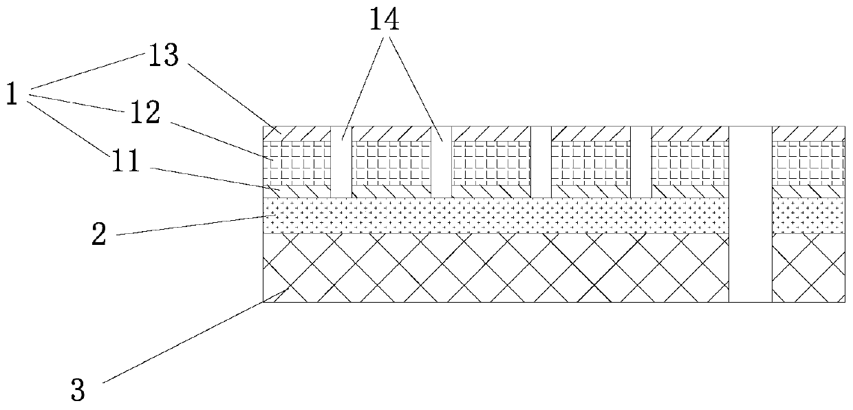
[0021] Such as figure 1 As shown, a double-layer single-sided copper-based circuit board. The manufacturing process of a double-layer single-sided copper-based circuit board includes the following steps a to e.

[0022] Step a, cutting according to the process size to obtain FR4 board 1, FR4 board 1 includes FR4 core material layer 12, copper layers arranged on both sides of FR4 core material layer, FR4 board 1 is baked, the temperature of the baked board is 135~165°C, The baking time is 3.6~4.5h; copper is deposited on one side of the FR4 board 1 to obtain a thickened inner copper layer.

[0023] The baking plate is thickened with a copper layer, and the thickened inner copper layer has a stable structure, is not easy to delaminate, and is not easy to cause copper skin and air bubbles; the inner layer circuit 11 has a stable str...


PUM


Abstract

The invention discloses a double-layer one-side copper-based circuit board making process comprising the following steps: baking a FR4 board, obtaining an internal layer line on the FR4 board, and silkprinting a solder mask on the internal layer line; stacking a plurality of slots and / or vias on a copper base, and placing a high temperature glue film or release film below slot / via on the copper base; laminating the FR4 board, a bonding sheet and the copper base at a high temperature; drilling blind holes on the FR4 board, electroplating copper on the FR4 board and etching same, thus obtainingan external layer line. The high temperature glue film or release film are placed on hollow positions before lamination, thus increasing lamination buffer force, and effectively preventing the soldermask from dropping oil under ununiform lamination of the board; the process can prevent the circuit board from layering and foaming via the board baking and pad high temperature lamination; a dry filmof 45-55 um is selected so as to fully cover the blind holes, thus preventing blind hole broken caused by developing and etching, and preventing the copper layer from being broken.

Description

technical field [0001] The invention relates to a circuit board, in particular to a manufacturing process of a double-layer single-side copper-based circuit board. Background technique [0002] In the ordinary MPCB double-layer one-sided lamination process, it is sufficient to laminate FR4 and the metal base. Adopting ordinary pressed copper-based hollow board process will result in poor reliability and easy layering and blistering; the FR4 panel will lose oil to a large extent after pressing; when making circuit film, there will be a large area of ​​serious holes after development, which will lead to The copper layer of the blind via is cracked. Contents of the invention [0003] In order to overcome the deficiencies of the prior art, the object of the present invention is to provide a manufacturing process for a double-layer single-side copper-based circuit board, so as to improve the quality of the circuit board. [0004] The technical scheme that the present inventio...

Claims


Application Information

Patent Timeline
Patent Type & Authority Patents(China)
IPC IPC(8): H05K3/00H05K3/28
CPCH05K3/0094H05K3/281H05K2203/111
Inventor 徐建华
Owner ZHUHAI KINGROAD ELECTRONICS
Why Eureka
Try Eureka