Auxiliary electrode transfer structure and manufacturing method of display panel

An auxiliary electrode and transfer structure technology, applied in circuits, electrical components, electrical solid devices, etc., can solve the problem of uneven brightness of display panels, and achieve the effects of improving adverse effects, improving uneven brightness, and simple methods.

Inactive Publication Date: 2019-08-20
SHENZHEN CHINA STAR OPTOELECTRONICS SEMICON DISPLAY TECH CO LTD
View PDF5 Cites 0 Cited by
  • Summary
  • Abstract
  • Description
  • Claims
  • Application Information

AI Technical Summary

Problems solved by technology

[0005] In order to solve the above-mentioned technical problems: the present invention provides an auxiliary electrode transfer structure and a method for manufacturing a display panel. The auxiliary electrode is transferred to the electrodes in the display panel through the auxiliary electrode transfer structure, so as to improve the defects caused by the transfer of the existing auxiliary electrodes. At the same time, it improves the uneven brightness of the display panel caused by the voltage drop caused by the high sheet resistance of the cathode

Method used


Image

  • Auxiliary electrode transfer structure and manufacturing method of display panel
  • Auxiliary electrode transfer structure and manufacturing method of display panel
  • Auxiliary electrode transfer structure and manufacturing method of display panel

Examples


Embodiment Construction

[0033] The following description of the embodiments refers to the accompanying drawings to illustrate specific embodiments in which the invention may be practiced. The directional terms mentioned in the present invention, such as "up", "down", "front", "back", "left", "right", "top", "bottom", etc., are only for reference to the attached drawings. direction. Therefore, the directional terms used are used to illustrate and understand the present invention, but not to limit the present invention.

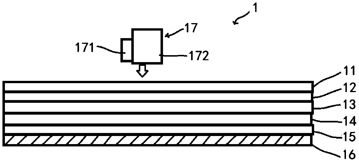
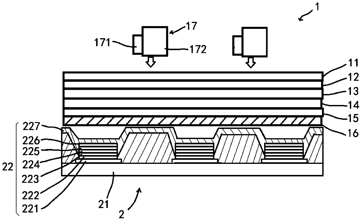
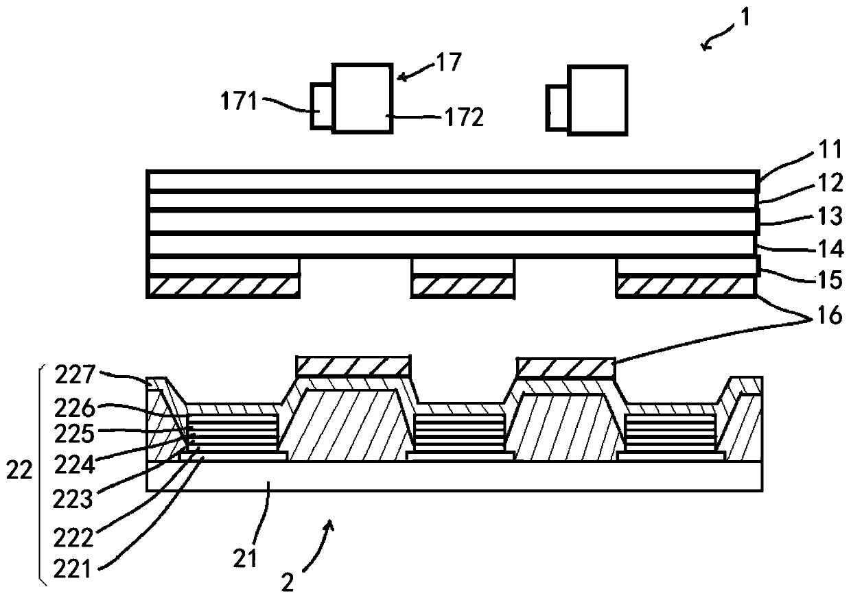
[0034] like figure 1 As shown, in one embodiment, an auxiliary electrode transfer structure 1 of the present invention includes a transparent base layer 11, a barrier layer 12, a light-to-heat conversion layer 13, a graphene layer 14, an intermediate layer 15, an auxiliary electrode 16 and a laser mechanism 17.

[0035] The transparent base layer 11 can be selected from transparent glass or transparent plastic.

[0036] The barrier layer 12 is disposed on the transparent base laye...


PUM


Abstract

The invention discloses an auxiliary electrode transfer structure and a manufacturing method of a display panel. The auxiliary electrode transfer structure comprises a transparent base layer; a photo-thermal conversion layer arranged on the transparent base layer; an auxiliary electrode arranged on the photo-thermal conversion layer; and a laser mechanism used for forming laser which penetrates through the transparent base layer to reach the photo-thermal conversion layer. According to the auxiliary electrode transfer structure and the manufacturing method of the display panel, the auxiliary electrode can be effectively transferred to the cathode of an OLED device through the auxiliary electrode transfer structure; adverse effects generated during transfer of the existing auxiliary electrode are effectively improved; and the phenomenon of uneven brightness of the display panel caused by the voltage drop generated by high square resistance of the cathode is effectively improved.

Description

technical field [0001] The invention relates to the field of display technology, in particular to an auxiliary electrode transfer structure and a manufacturing method of a display panel. Background technique [0002] AMOLED display devices can be classified into bottom emission type (light is emitted from the side of the array substrate) and top emission type (light is emitted from the side of the package cover glass). In the top-emitting AMOLED display device, because the light source of the OLED needs to penetrate the cathode of the OLED, a transparent or semi-transparent cathode material must be used. In the prior art, transparent cathode materials mostly use transparent oxides (TCO, such as IZO). The thickness range of TCO is between 100nm and 500nm, and the sheet resistance is between 5 and 30Ω / □. Semi-transparent cathodes mostly use thin metals (such as silver, silver-magnesium alloy, etc.), in order to maintain a light transmittance of more than 40% for semi-transpar...

Claims


Application Information

Patent Timeline
Patent Type & Authority Applications(China)
IPC IPC(8): H01L51/52H01L51/56H01L21/77
CPCH01L21/77H10K71/60H10K59/80522H10K71/621H10K50/824
Inventor 方俊雄
Owner SHENZHEN CHINA STAR OPTOELECTRONICS SEMICON DISPLAY TECH CO LTD
Why Eureka
Try Eureka