Check patentability & draft patents in minutes with Patsnap Eureka AI!

Organic light-emitting diode display

A light-emitting diode and display technology, which is applied in the manufacture of electric solid-state devices, semiconductor devices, semiconductor/solid-state devices, etc., can solve the problems that the cathode voltage drop affects the luminous brightness of the display panel, and achieve the effect of improving the resistance voltage drop

Active Publication Date: 2019-08-27
SHENZHEN CHINA STAR OPTOELECTRONICS SEMICON DISPLAY TECH CO LTD
View PDF10 Cites 12 Cited by
  • Summary
  • Abstract
  • Description
  • Claims
  • Application Information

AI Technical Summary

Problems solved by technology

[0004] The purpose of this application is to provide an organic light emitting diode display to solve the problem that the luminous brightness of the display panel is affected by the excessive cathode voltage drop when the top-emission display panel is manufactured as a large-size display panel

Method used


Image

  • Organic light-emitting diode display
  • Organic light-emitting diode display
  • Organic light-emitting diode display

Examples


Embodiment Construction

[0036] The technical solutions in the embodiments of the present application will be clearly and completely described below in conjunction with the drawings in the embodiments of the present application. Apparently, the described embodiments are only some of the embodiments of this application, not all of them. Based on the embodiments in this application, all other embodiments obtained by those skilled in the art without making creative efforts belong to the scope of protection of this application.

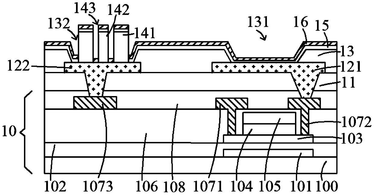
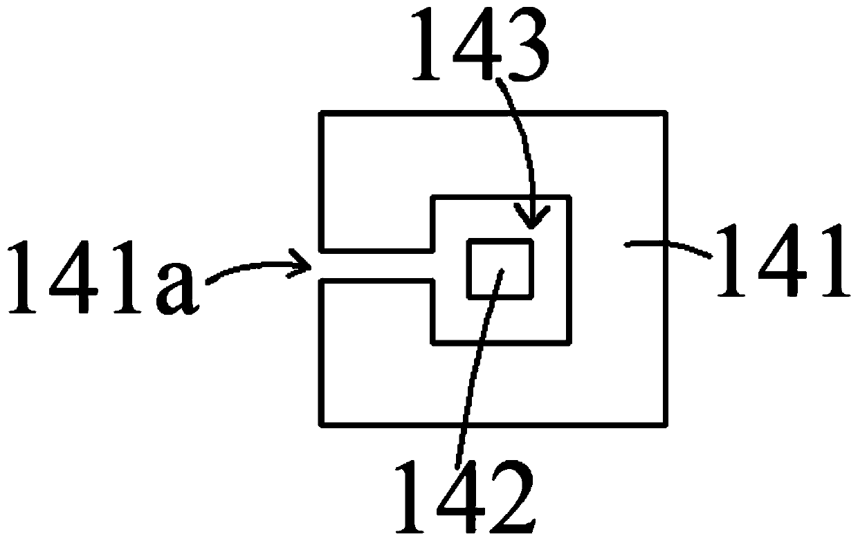
[0037] see figure 1 , which is a schematic diagram of the first structure of an organic light emitting diode display according to an embodiment of the present application. The OLED display includes a substrate 10 , an auxiliary electrode, a planarization layer 11 , an anode 121 , a pixel definition layer 13 , cathode isolation columns, an organic functional layer 15 and a cathode 16 .

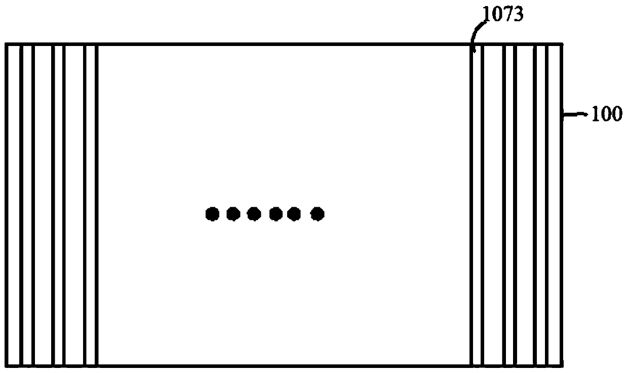
[0038] The substrate is a thin film transistor array substrate. The thin film transistor arr...


PUM


Abstract

The invention provides an organic light-emitting diode display. A contact hole is formed in a negative electrode isolation post, a negative electrode is formed on an auxiliary electrode in the contacthole, the negative electrode in the contact hole is electrically connected with the auxiliary electrode, the negative electrode in the contact hole is connected with a negative electrode outside thenegative electrode isolation post by a third opening in a side surface of the negative electrode isolation post, the problem of resistance drop of the negative electrode in a large-size display panelis solved, and the problem that light-emitting brightness of a large-size top light-emitting display panel is affected due to large resistance drop of the negative electrode is solved.

Description

technical field [0001] The present application relates to the field of display technology, in particular to an organic light emitting diode display. Background technique [0002] Currently, Organic Light Emitting Diode (OLED) displays include top emission (Top Emission), bottom emission (Bottom Emission) and transparent display (Transparent Display) and other light emitting methods. Among them, the top-emitting OLED display has the advantages of high resolution and large light-emitting area, and is widely used in small-sized OLED display panels. Since large-size display panels tend to increase resolution, top-emission display panels have become an important research direction for large-size display panels. When the top-emitting display panel is manufactured as a large-size display panel, the cathode material is required to be transparent and the thickness of the cathode should not be too large, so as to ensure the light output rate of the OLED display panel. Due to the thi...

Claims


Application Information

Patent Timeline
Patent Type & Authority Applications(China)
IPC IPC(8): H01L27/32H01L51/52
CPCH10K59/1315H10K50/824
Inventor 聂诚磊
Owner SHENZHEN CHINA STAR OPTOELECTRONICS SEMICON DISPLAY TECH CO LTD
Features
  • R&D
  • Intellectual Property
  • Life Sciences
  • Materials
  • Tech Scout
  • Unparalleled Data Quality
  • Higher Quality Content
  • 60% Fewer Hallucinations
Learn More