Display panel, manufacturing method thereof, and display device
A technology for display panels and manufacturing methods, applied in semiconductor/solid-state device manufacturing, semiconductor devices, electrical components, etc., can solve problems such as poor edge uniformity, achieve the effect of reducing the difference in dryness and meeting the requirements of narrow frame design
- Summary
- Abstract
- Description
- Claims
- Application Information
AI Technical Summary
Problems solved by technology
Method used
Image

Examples
Embodiment 1
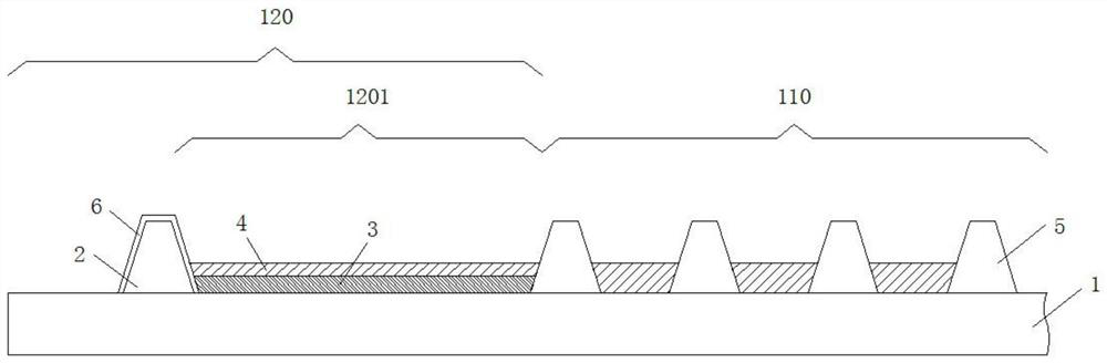
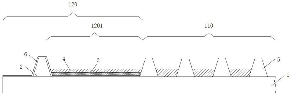
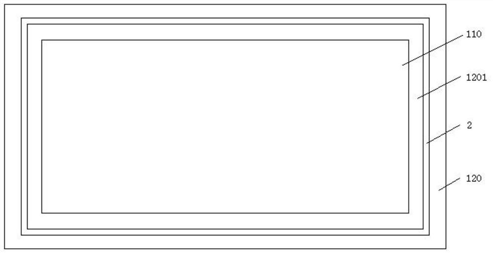
[0037] Such as Figure 1-Figure 3 As shown, Embodiment 1 of the present invention proposes a display panel, including a display substrate 1. The display substrate 1 includes a display area 110 and a non-display area 120 surrounding the display area 110, and further includes:
[0038] The test area 1201, the test area 1201 is set in the non-display area 120, and surrounds the edge of the display area 110, and is used for inkjet printing at the same time as the display area 110; the retaining wall 2, the retaining wall 2 is arranged outside the test area 1201 Edge; sacrificial layer 3, the sacrificial layer 3 is arranged on the test area 1201 and is located in the area surrounded by the retaining wall 2, for forming and separating the printing film layer 4 formed by inkjet printing; wherein, the test area 1201 and the non-display area 120 corresponding to the package area.
[0039] Wherein, the display substrate 1 includes a display area 110 for display, and a non-display area ...
Embodiment 2
[0046] Such as Figure 4-Figure 6 As shown, Embodiment 2 of the present invention proposes a method for manufacturing a display panel, including:
[0047] S1: setting the test area 1201 and the retaining wall 2 surrounding the outer edge of the test area 1201 in the non-display area 120 of the display substrate 1;
[0048] Specifically, during manufacture, a test area 1201 is preset in the non-display area 120 of the display substrate 1, the test area 1201 surrounds the periphery of the display area 110, and the test area 1201 is displayed by setting a retaining wall 2 on the periphery of the test area 1201. range, and can prevent ink droplets from spreading to areas other than the test area 1201 during inkjet printing. The range of the preset test area 1201 is set corresponding to the encapsulation area of the display substrate 1 . When setting, the area of the test area 12011 may not be larger than the encapsulation area of the non-display area 120 . S2: forming a sa...
Embodiment 3
[0061] Embodiment 3 of the present invention provides a display device, including the above-mentioned display panel.
[0062] Specifically, the display device may be an electronic device with a display function such as a television, a mobile phone, and a tablet computer.
[0063] Embodiment 3 of the present invention proposes a display device. By setting a test area, the inkjet printing coverage of the display substrate can be increased, thereby reducing the difference in dryness between the middle part and the edge part of the display area of the display substrate, and solving the problem of the display substrate. The problem of poor uniformity of the printing film layer at the edge of the printing area of the display area can ensure the display effect of the display device; by setting a sacrificial layer in the test area, the sacrificial layer can play a role in the test area after inkjet printing forms a printing film layer. The function of assisting the removal of the ...
PUM
 Abstract
Description
Claims
Application Information
 - Generate Ideas
- Intellectual Property
- Life Sciences
- Materials
- Tech Scout
- Unparalleled Data Quality
- Higher Quality Content
- 60% Fewer Hallucinations
Browse by: Latest US Patents, China's latest patents, Technical Efficacy Thesaurus, Application Domain, Technology Topic, Popular Technical Reports.
© 2025 PatSnap. All rights reserved.Legal|Privacy policy|Modern Slavery Act Transparency Statement|Sitemap|About US| Contact US: help@patsnap.com