OLED display device and manufacturing method
A technology for a display device and a manufacturing method, applied in identification devices, instruments, calculations, etc., can solve the problems of unfavorable small electronic equipment design, increased frame size, easy wear, etc., shorten communication distance, reduce module thickness, The effect of reducing production costs
- Summary
- Abstract
- Description
- Claims
- Application Information
AI Technical Summary
Problems solved by technology
Method used
Image

Examples
no. 1 example
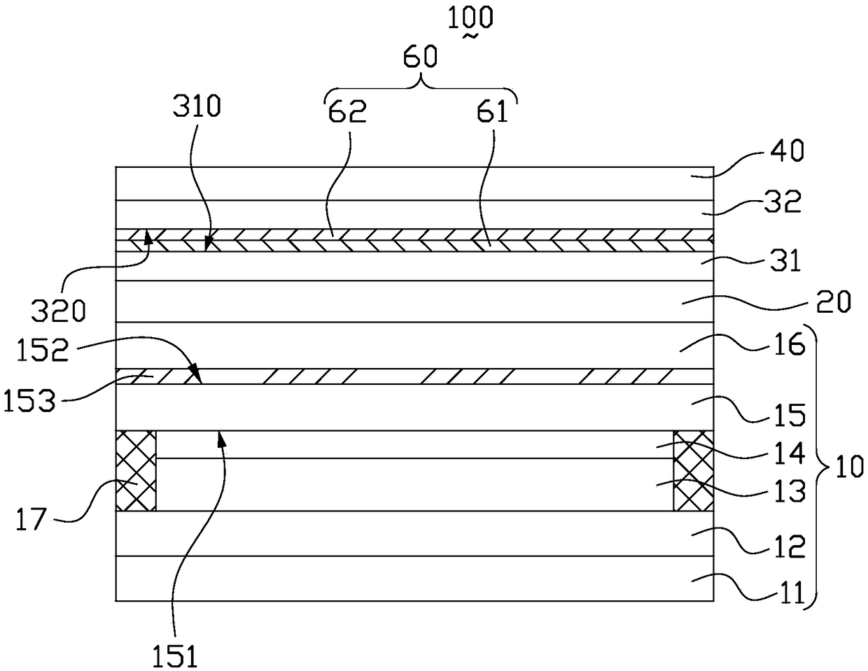
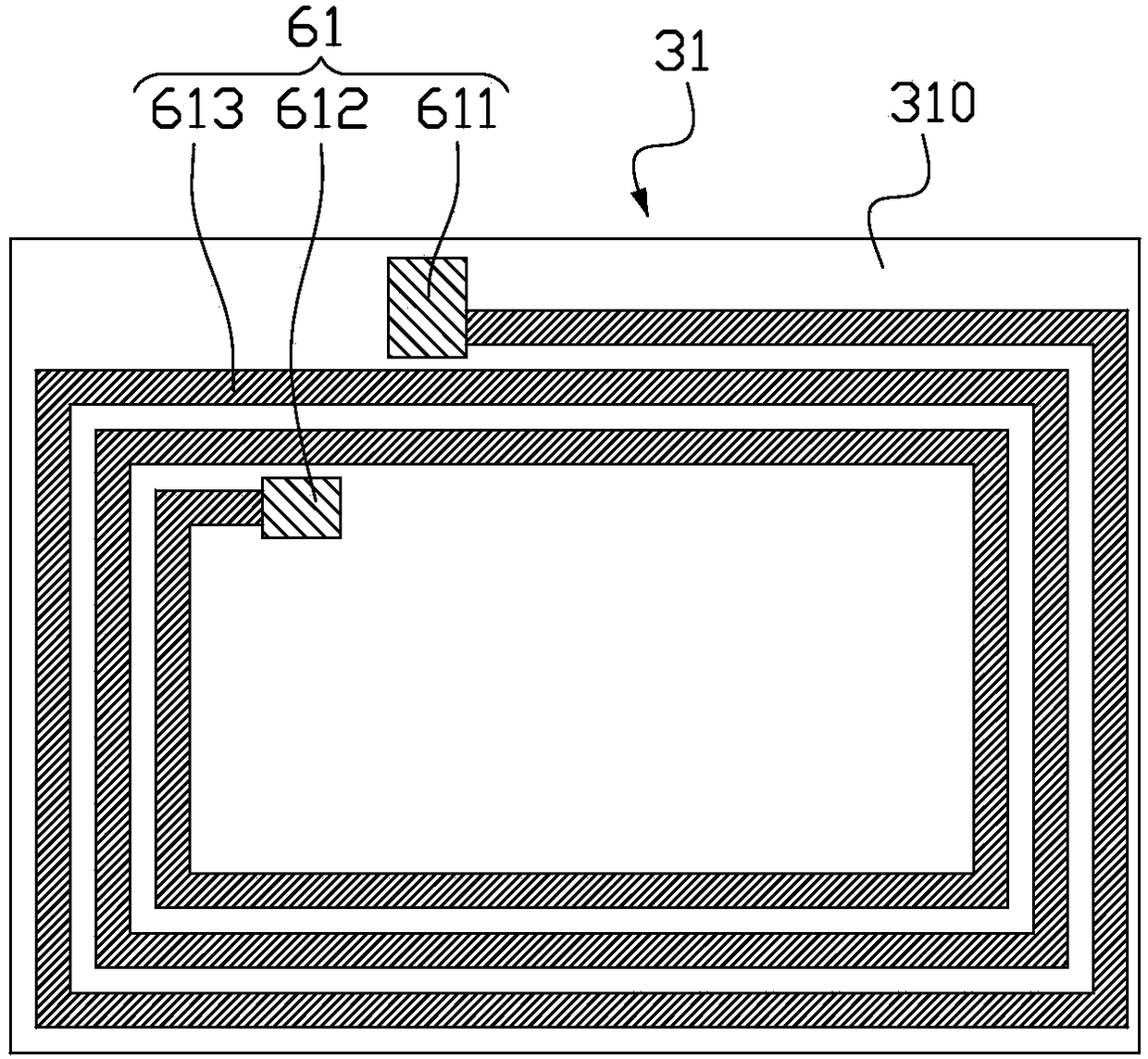
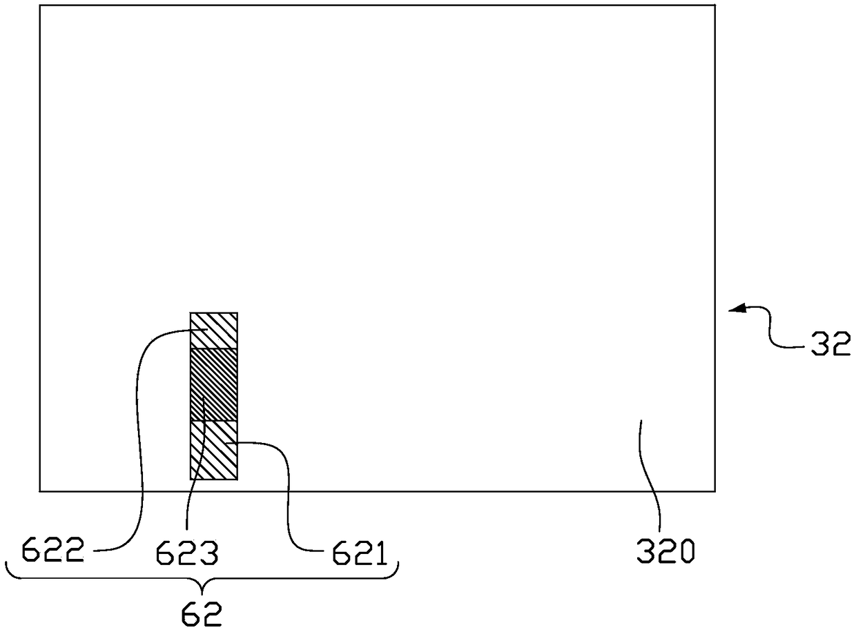
[0048] figure 1 It is a schematic structural diagram of the OLED display device in the first embodiment of the present invention, please refer to figure 1 , the OLED display device 100 includes an OLED display panel 10, an isolation layer 20, a first transparent film 31, a second transparent film 32, and a cover glass 40. In this embodiment, the display panel 10, the isolation layer 20, the first transparent film The film 31, the second transparent film 32 and the cover glass 40 are stacked in sequence, that is, the isolation layer 20 is disposed on the OLED display panel 10, the first transparent film 31 is disposed on the isolation layer 20, and the second transparent film 32 is disposed on the first On the transparent film 31 , the cover glass 40 is disposed on the second transparent film 32 , and the various structural layers can be bonded by transparent optical adhesive (OCA). In other embodiments, the positions of the first transparent film 31 and the second transparent...
no. 2 example
[0060] Figure 4 It is a schematic structural diagram of the OLED display device in the second embodiment of the present invention, please refer to Figure 4, the OLED display device 100a includes an OLED display panel 10, an isolation layer 20, a transparent film 33, and a cover glass 40. In this embodiment, the display panel 10, the isolation layer 20, the transparent film 33, and the cover glass 40 are stacked in sequence. That is, the isolation layer 20 is disposed on the OLED display panel 10 , the transparent film 33 is disposed on the isolation layer 20 , the cover glass 40 is disposed on the transparent film 33 , and the various structural layers can be bonded by transparent optical adhesive (OCA).
[0061] The OLED display panel 10 includes an OLED panel encapsulation cover 11 , an OLED first electrode 12 , an OLED light-emitting area 13 , an OLED second electrode 14 , an OLED substrate 15 and an insulating protection film 16 which are sequentially stacked. When the ...
no. 3 example
[0066] Figure 7 It is a schematic structural diagram of the display device in the third embodiment of the present invention, please refer to Figure 7 , the OLED display device 100b includes an OLED display panel 10, an isolation layer 20, a transparent film 34, and a cover glass 40. In this embodiment, the display panel 10, the isolation layer 20, the transparent film 34, and the cover glass 40 are stacked in sequence That is, the isolation layer 20 is disposed on the OLED display panel 10 , the transparent film 34 is disposed on the isolation layer 20 , the cover glass 40 is disposed on the transparent film 34 , and the various structural layers can be bonded by transparent optical adhesive (OCA).
[0067] The OLED display panel 10 includes an OLED panel encapsulation cover 11 , an OLED first electrode 12 , an OLED light-emitting area 13 , an OLED second electrode 14 , an OLED substrate 15 and an insulating protection film 16 which are sequentially stacked. When the OLED d...
PUM
 Abstract
Description
Claims
Application Information
 - Generate Ideas
- Intellectual Property
- Life Sciences
- Materials
- Tech Scout
- Unparalleled Data Quality
- Higher Quality Content
- 60% Fewer Hallucinations
Browse by: Latest US Patents, China's latest patents, Technical Efficacy Thesaurus, Application Domain, Technology Topic, Popular Technical Reports.
© 2025 PatSnap. All rights reserved.Legal|Privacy policy|Modern Slavery Act Transparency Statement|Sitemap|About US| Contact US: help@patsnap.com