

Drive circuit, matrix substrate, and display device
A technology for driving circuits and matrix substrates, which can be applied to circuits, identification devices, electrical components, etc., and can solve the problems of reduced mechanical strength and easy breakage of wiring.
- Summary
- Abstract
- Description
- Claims
- Application Information
AI Technical Summary
Problems solved by technology
Method used
Image

Examples
Embodiment approach 1
[0037] Next, Embodiment 1 of the present invention will be described in detail.
[0038] (Constitution of Matrix Substrate)
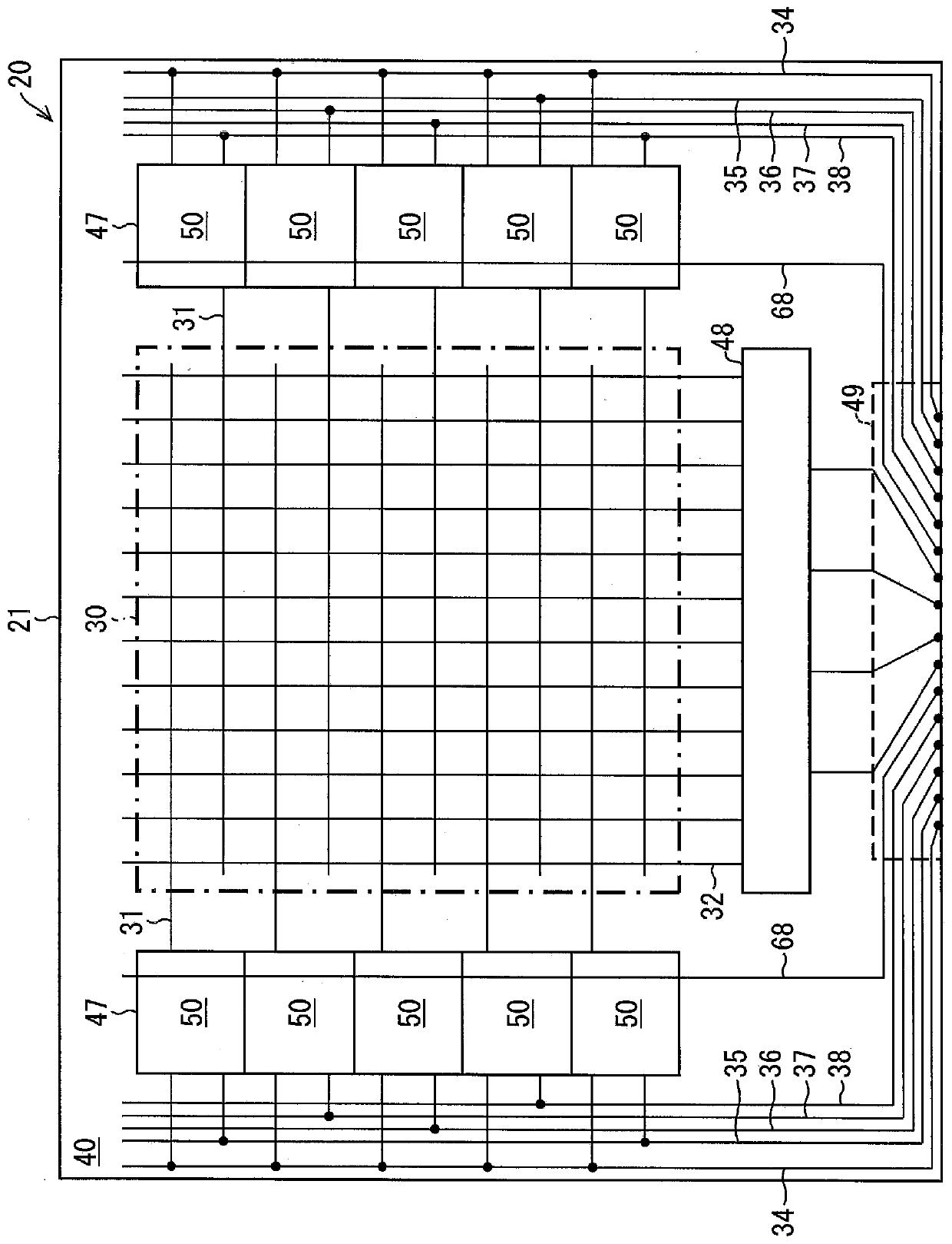
[0039] figure 1 It is a plan view showing a schematic configuration of the matrix substrate 20 including the scanning line driving circuit 47 according to Embodiment 1 of the present invention.
[0040] Such as figure 1 As shown, the matrix substrate 20 includes an insulating substrate 21 , and the insulating substrate 21 has a display area 30 and a peripheral area 40 other than the display area 30 on its upper surface.
[0041] In the display area 30 , a plurality of scanning lines 31 (output lines) and a plurality of data lines 32 are arranged in a grid pattern. Also, while in figure 1 Not shown in , but other structures such as pixel transistors and pixel electrodes are also arranged in the display region 30 .
[0042] In the peripheral region 40 are arranged: a scanning line driving circuit 47 (driving circuit), which includes a plurality of...
Embodiment approach 2
[0168] based on Figure 15 ~ Figure 16 Another embodiment of the present invention will be described below. In addition, for convenience of description, members having the same functions as those described in the above-mentioned embodiments are given the same reference numerals, and descriptions thereof are omitted.
[0169] The matrix substrate 20 of the second embodiment differs from the matrix substrate 20 of the first embodiment in the following two points, but has the same configuration as the matrix substrate 20 of the first embodiment except for these points. First, in Embodiment 2, unlike Embodiment 1, additional wiring layer 27 and second interlayer insulating film 28 are laminated between insulating substrate 21 and gate layer 22 . Second, in Embodiment 2, unlike Embodiment 1, no transition portion 71 is provided, and the wiring or electrodes formed by the gate layer 22 and the wiring or electrodes formed by the source layer 25 are directly connected. .
[0170] ...
Embodiment approach 3
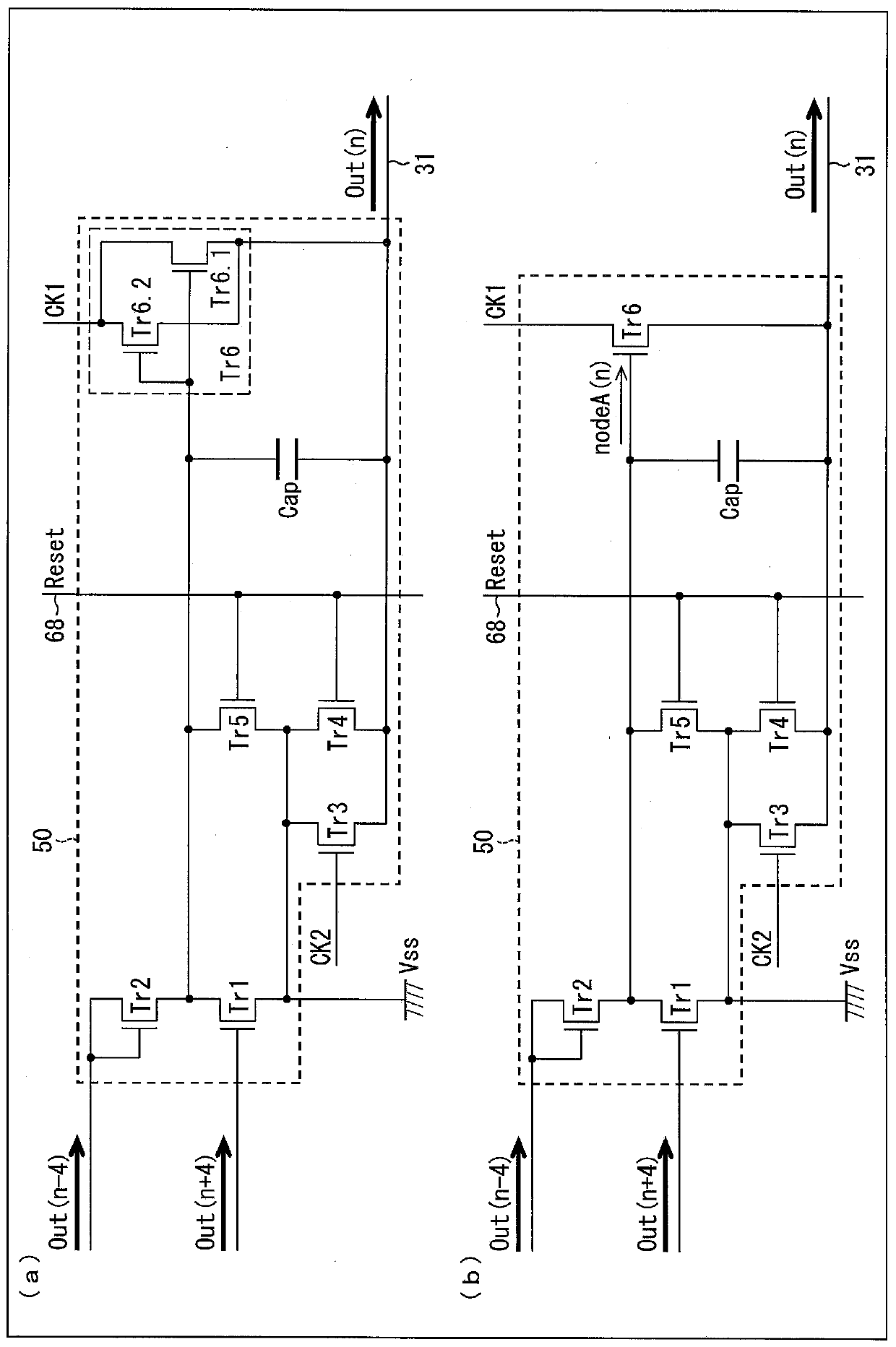
[0183] based on Figure 18 Another embodiment of the present invention will be described below. In addition, for convenience of description, members having the same functions as those described in the above-mentioned embodiments are given the same reference numerals, and descriptions thereof are omitted.
[0184] Figure 18 It is a plan view showing a schematic circuit configuration of a unit circuit 50 according to the third embodiment.
[0185] In the matrix substrate 20 of the third embodiment, compared with the matrix substrate 20 of the first embodiment, the arrangement of the first transistor Tr1 and the first relay wiring 66 is changed according to the change of the shape of the sixth transistor Tr6 . Except for this, the matrix substrate 20 of the third embodiment has the same configuration as the matrix substrate 20 of the first embodiment.
[0186] Such as Figure 18 As shown, the sixth transistor Tr6 in the third embodiment is divided by the first relay line 66 ...
PUM
 Abstract
Description
Claims
Application Information