
A light emitting diode display

A technology for light-emitting diodes and displays, applied in semiconductor devices, electric solid-state devices, electrical components, etc., can solve problems such as large-area transfer and low efficiency, achieve high matching accuracy, solve massive transfer, and improve assembly efficiency.

Active Publication Date: 2021-10-01
SHENZHEN SITAN TECH CO LTD
View PDF4 Cites 0 Cited by
  • Summary
  • Abstract
  • Description
  • Claims
  • Application Information

AI Technical Summary

Problems solved by technology

The traditional "grab and release" method is too inefficient to transfer a large area in a short time, and the efficiency is low

Method used


Image

  • A light emitting diode display
  • A light emitting diode display
  • A light emitting diode display

Examples


Embodiment 1

[0037] Miniaturization process technology and mass transfer technology are the core processes of the Micro-LED transfer process, among which the miniaturization process technology is to miniaturize, array and thin-film the traditional LED crystal film. Mass transfer technology is to transfer miniaturized and arrayed LED crystal films to circuit boards in batches. Arrange the miniature light-emitting diode chips smaller than 100 microns in matrix, and then transfer them to the circuit board in batches by mass transfer technology, and then package them to form a whole LED panel.

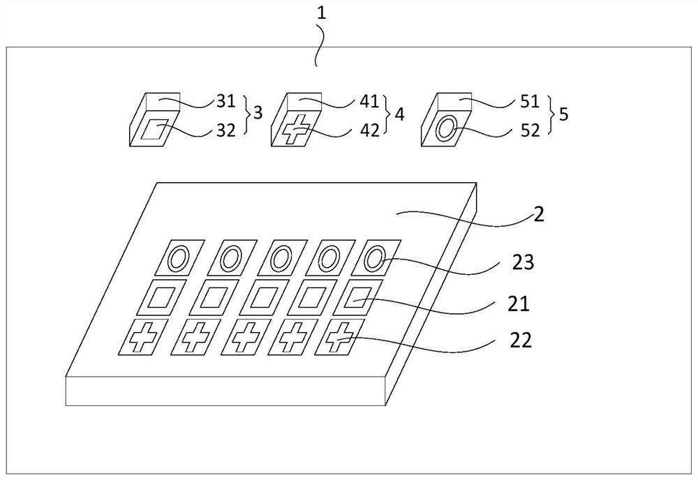
[0038] Such as figure 1 As shown, a light emitting diode display 1 is provided in this embodiment, and the light emitting diode display 1 of this embodiment is a color display.

[0039] The light emitting diode display 1 of this embodiment includes a circuit substrate 2 and a plurality of light emitting diodes. The plurality of light emitting diodes in this embodiment include a first light emitting d...

Embodiment 2

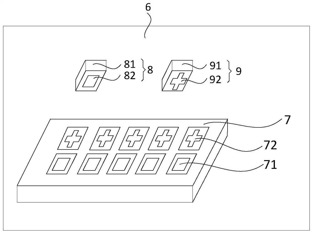
[0056] Such as figure 2 As shown, a light emitting diode display 6 is provided in this embodiment, and the light emitting diode display 6 is a monochrome display.

[0057] The LED display 6 of this embodiment includes a circuit substrate 7 and a plurality of LEDs. The plurality of light emitting diodes in this embodiment include a first light emitting diode 8 and a second light emitting diode 9 . Each light emitting diode includes a light emitting diode chip and a patterned first magnetic electrode layer, the first magnetic electrode layer being the anode and / or the cathode of the light emitting diode chip.

[0058] Specifically, the first LED 8 includes a red LED chip 81 and a seventh electrode pattern 82 , and the second LED 9 includes a green LED chip 91 and an eighth electrode pattern 92 . In this embodiment, for example, the seventh electrode pattern 82 is square, and the eighth electrode pattern 92 is cross-shaped. Optionally, the light emitting diodes may also be: t...

Embodiment 3

[0064] This embodiment provides various electrode patterns of the first magnetic electrode layer and the second magnetic electrode layer, which are used in the case where at least two kinds of diode chips are assembled at the same time. By designing different electrode patterns, at least two color devices can be matched at the same time, without the need for multiple transfers. At the same time, by designing special electrode patterns, the difference between electrode patterns is large and the coincidence is small to achieve higher The matching accuracy greatly improves the efficiency and yield of the assembly process.

[0065] In the assembly process of this embodiment, the following assembly situations are included: the red light diode chip and the blue light diode chip are assembled at the same time, the blue light diode chip and the green light diode chip are assembled at the same time; the red light diode chip and the green light diode chip are assembled at the same time; ...


PUM


Abstract

The invention discloses a light-emitting diode display, comprising: a plurality of light-emitting diodes, each light-emitting diode includes a light-emitting diode chip and a patterned first magnetic electrode layer, and the first magnetic electrode layer is the anode of the light-emitting diode chip and / or Or the negative electrode; a circuit substrate for driving multiple light emitting diodes, the circuit substrate includes a plurality of patterned second magnetic electrode layers arranged in a matrix, and the second magnetic electrode layer is used for absorbing and connecting the light emitting diodes. On the basis of not affecting the structure of the original device, the invention solves the problem of mass transfer, achieves higher matching accuracy and improves assembly efficiency.

Description

technical field [0001] The embodiment of the present invention relates to an LED assembly technology, in particular to a light emitting diode display. Background technique [0002] Micro-LED is a new generation of display technology. Compared with the existing liquid crystal display, it has higher photoelectric efficiency, higher brightness, higher contrast ratio, and lower power consumption, and can also be combined with a flexible panel to realize flexible display. Compared with traditional LEDs, it has the same light-emitting principle, but the scale of a single LED is less than 20 μm, which greatly increases the difficulty of its preparation. In the preparation process, mass transfer technology is the key. [0003] In order to accommodate large-area displays, a large number of LEDs need to be transferred from the sapphire substrate to the glass plate. The traditional "grab and release" method is too inefficient to transfer large areas in a short time, and the efficien...

Claims


Application Information

Patent Timeline
Patent Type & Authority Patents(China)
IPC IPC(8): H01L27/15H01L33/62H01L33/38
CPCH01L27/156H01L33/38H01L33/62
Inventor 刘召军容沃铖罗冰清
Owner SHENZHEN SITAN TECH CO LTD
Learn More