
Structure of vertical type light emitting diode grain and manufacturing method of vertical type light emitting diode grains

A technology of light-emitting diodes and manufacturing methods, which is applied in the direction of electrical components, circuits, semiconductor devices, etc., and can solve problems such as poor thermal expansion coefficient, bending and deformation of substrates, and affecting the luminous efficiency of LED chips

Active Publication Date: 2019-06-04
INGENTEC CORP
View PDF3 Cites 0 Cited by
  • Summary
  • Abstract
  • Description
  • Claims
  • Application Information

AI Technical Summary

Problems solved by technology

[0004] However, general LEDs are widely used nowadays, for example, they can be used in smart phones. Once the smart phone is overheated, it will also affect the LED chips installed in it, which will also affect the LED chips used to place the die. For substrates connected to smartphones or other devices, if the thermal expansion coefficient of the substrate is not good, it is easy to cause the substrate to bend and deform due to temperature changes, thereby affecting the luminous efficiency of the LED chip

Method used

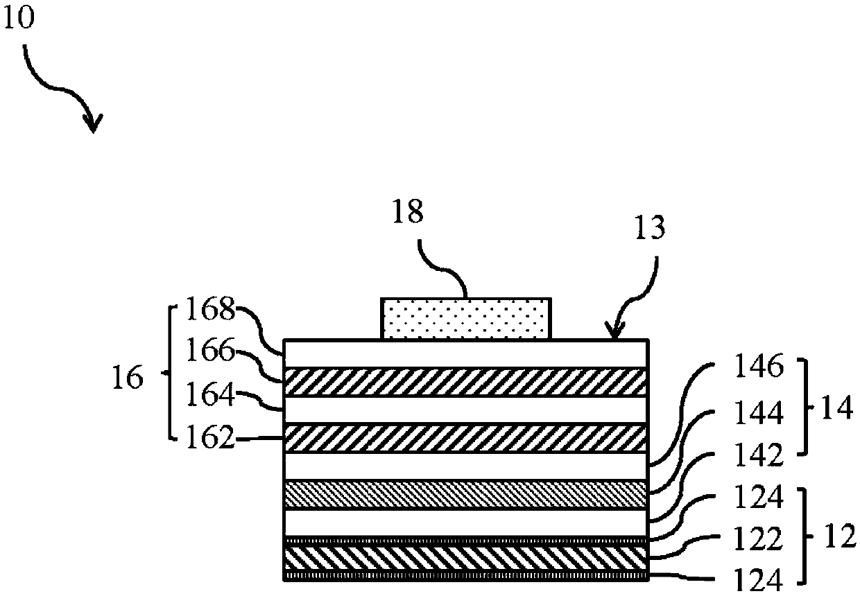
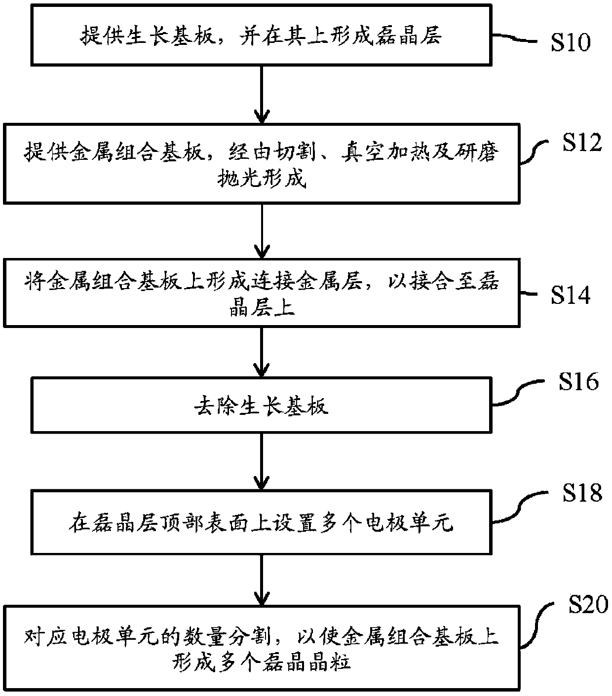

Image

  • Structure of vertical type light emitting diode grain and manufacturing method of vertical type light emitting diode grains
  • Structure of vertical type light emitting diode grain and manufacturing method of vertical type light emitting diode grains
  • Structure of vertical type light emitting diode grain and manufacturing method of vertical type light emitting diode grains

Examples


Embodiment Construction

[0058] The following will clearly and completely describe the technical solutions in the embodiments of the present invention with reference to the accompanying drawings in the embodiments of the present invention. Obviously, the described embodiments are only some, not all, embodiments of the present invention. Based on the embodiments of the present invention, all other embodiments obtained by persons of ordinary skill in the art without making creative efforts belong to the protection scope of the present invention.

[0059] In order to stabilize and improve the luminous efficiency of LEDs and effectively apply them to vertical LEDs, the present invention changes the thermal expansion coefficient of the substrate under the grains and improves heat conduction by improving the structure of the grains and the manufacturing method, so that the LEDs will be used at higher temperatures in the future. Under the environment, the luminous intensity will not change due to the deformat...


PUM

PropertyMeasurementUnit
Thicknessaaaaaaaaaa

Abstract

The invention provides a structure of a vertical type light emitting diode grain and a manufacturing method of vertical type light emitting diode grains. The method comprises a step of providing a growth substrate and growing an epitaxial layer on the growth substrate, a step of connecting a metal combination substrate to the epitaxial layer, a step of removing the growth substrate, a step of setting a plurality of electrode units on the top of the crystal layer, and a step of correspondingly dividing the epitaxial layer to form a plurality of epitaxial grains. The structure of each vertical type light emitting diode grain formed by the method comprises the metal combination substrate with a first metal layer and second metal layers on upper and lower surfaces of the first metal layer, andan epitaxial electrode layer located on the metal composite substrate, wherein the first metal layer and the second metal layer are combined by cutting, vacuum heating and grinding and polishing, themetal combination substrate provided by the invention has a high heat conduction coefficient, a low thermal expansion coefficient and initial permeability, and the formed light emitting diode grainsare more competitive.

Description

technical field [0001] The present invention relates to a light-emitting diode grain structure and its manufacturing method, in particular to a vertical light-emitting diode grain structure with high thermal conductivity, low thermal expansion coefficient and initial magnetic permeability and its manufacturing method. Background technique [0002] A light emitting diode (Light Emitting Diode, LED) is a light source made by semiconductor technology, which is formed by three and five (III-V) compound semiconductors. The principle of LED light emission is to use the combination of electrons and holes in the semiconductor to emit photons. Unlike traditional light bulbs that need to operate at a high temperature of thousands of degrees, and do not need to use high voltage to excite electron beams like fluorescent lamps, LEDs are the same as ordinary electronic components, only needing a voltage of 2 to 4 volts (V), and at normal temperatures It can operate normally, so the lumino...

Claims


Application Information

Patent Timeline
IPC IPC(8): H01L33/00H01L33/62
Inventor 陈亚理王起明涂家玮钟承育冯祥铵
Owner INGENTEC CORP
Learn More