

Light emitting diode display
A technology for light-emitting diodes and displays, which is applied to electric solid-state devices, semiconductor devices, electrical components, etc., can solve problems such as low efficiency and large-area transfer, and achieve the effect of solving massive transfer, high matching accuracy, and improving assembly efficiency.
- Summary
- Abstract
- Description
- Claims
- Application Information
AI Technical Summary
Problems solved by technology
Method used
Image

Examples
Embodiment 1
[0037] Miniaturization process technology and mass transfer technology are the core processes of the Micro-LED transfer process, among which the miniaturization process technology is to miniaturize, array and thin-film the traditional LED crystal film. Mass transfer technology is to transfer miniaturized and arrayed LED crystal films to circuit boards in batches. Arrange the miniature light-emitting diode chips smaller than 100 microns in matrix, and then transfer them to the circuit board in batches by mass transfer technology, and then package them to form a whole LED panel.
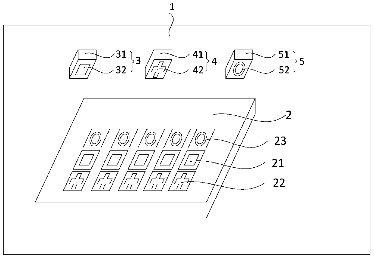
[0038] Such as figure 1 As shown, a light emitting diode display 1 is provided in this embodiment, and the light emitting diode display 1 of this embodiment is a color display.
[0039] The light emitting diode display 1 of this embodiment includes a circuit substrate 2 and a plurality of light emitting diodes. The plurality of light emitting diodes in this embodiment include a first light emitting d...
Embodiment 2
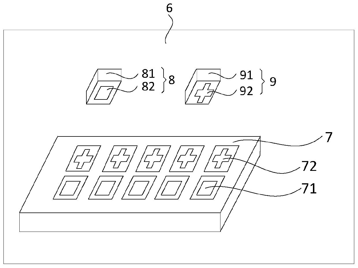
[0056] Such as figure 2 As shown, a light emitting diode display 6 is provided in this embodiment, and the light emitting diode display 6 is a monochrome display.
[0057] The LED display 6 of this embodiment includes a circuit substrate 7 and a plurality of LEDs. The plurality of light emitting diodes in this embodiment include a first light emitting diode 8 and a second light emitting diode 9 . Each light emitting diode includes a light emitting diode chip and a patterned first magnetic electrode layer, the first magnetic electrode layer being the anode and / or the cathode of the light emitting diode chip.
[0058] Specifically, the first LED 8 includes a red LED chip 81 and a seventh electrode pattern 82 , and the second LED 9 includes a green LED chip 91 and an eighth electrode pattern 92 . In this embodiment, for example, the seventh electrode pattern 82 is square, and the eighth electrode pattern 92 is cross-shaped. Optionally, the light emitting diodes may also be: t...
Embodiment 3
[0064] This embodiment provides various electrode patterns of the first magnetic electrode layer and the second magnetic electrode layer, which are used in the case where at least two kinds of diode chips are assembled at the same time. By designing different electrode patterns, at least two color devices can be matched at the same time, without the need for multiple transfers. At the same time, by designing special electrode patterns, the difference between electrode patterns is large and the coincidence is small to achieve higher The matching accuracy greatly improves the efficiency and yield of the assembly process.
[0065] In the assembly process of this embodiment, the following assembly situations are included: the red light diode chip and the blue light diode chip are assembled at the same time, the blue light diode chip and the green light diode chip are assembled at the same time; the red light diode chip and the green light diode chip are assembled at the same time; ...
PUM
 Abstract
Description
Claims
Application Information