
Method and System for Generating Circuit Schematic Diagram

A technology of circuit schematic diagram and constraint diagram, which is applied in the direction of electrical digital data processing, special data processing applications, instruments, etc., can solve the problems that are not suitable for the use of FPGA integrated circuits, etc., and achieve good graphical display effect, less connection crossing, The effect of less bending of the connecting line

Active Publication Date: 2020-12-25
SHANGHAI ANLOGIC INFOTECH CO LTD
View PDF6 Cites 0 Cited by
  • Summary
  • Abstract
  • Description
  • Claims
  • Application Information

AI Technical Summary

Problems solved by technology

In the prior art, a grid-based circuit diagram automatic generation method is adopted, and a device is placed in each grid interval, which is more suitable for circuits with little difference in the size of the graphical display device, so it is not suitable for FPGA integrated circuits or in graphics. Use when displaying hierarchical integrated circuit designs

Method used


Image

  • Method and System for Generating Circuit Schematic Diagram
  • Method and System for Generating Circuit Schematic Diagram

Examples


Embodiment Construction

[0046] In order to make the purpose, technical solutions and advantages of the present invention clearer, the technical solutions in the embodiments of the present invention will be clearly and completely described below in conjunction with the accompanying drawings of the present invention. Obviously, the described embodiments are part of the present invention Examples, not all examples. Based on the embodiments of the present invention, all other embodiments obtained by persons of ordinary skill in the art without creative efforts fall within the protection scope of the present invention. Unless otherwise defined, the technical terms or scientific terms used herein shall have the usual meanings understood by those skilled in the art to which the present invention belongs. As used herein, "comprising" and similar words mean that the elements or items appearing before the word include the elements or items listed after the word and their equivalents, without excluding other el...


PUM


Abstract

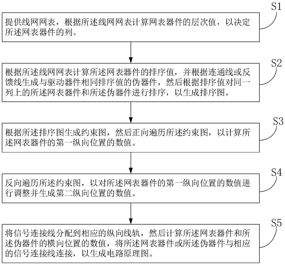
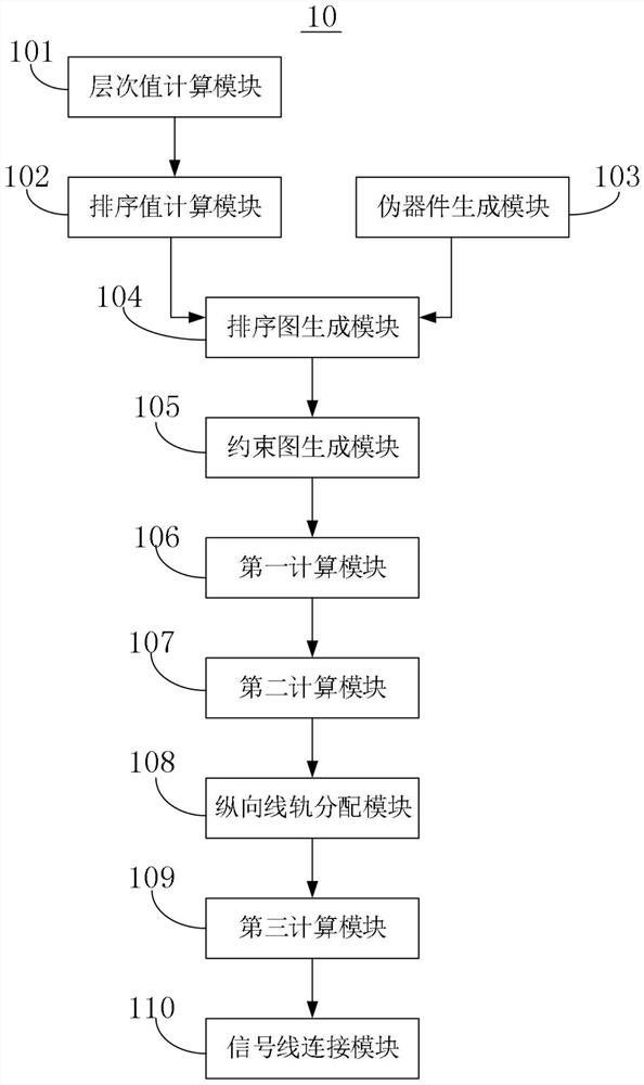
The invention provides a method for generating a schematic circuit diagram, which includes calculating the hierarchical value of the netlist device to determine the column of the netlist device, calculating the sorting value of the netlist device, and generating a pseudo-device according to the connection line or the feedback line. For the signal connection between adjacent devices, the wiring algorithm is simplified, and the netlist devices and pseudo-devices are sorted according to the sorting value to generate a sorting diagram, and the constraint diagram is generated according to the sorting diagram, with less wiring bends and forward traversal of the constraint diagram , calculate the value of the first vertical position, traverse the constraint graph in reverse, adjust the value of the first vertical position to generate the value of the second vertical position, assign the signal connection line to the vertical track, calculate the value of the horizontal position, and connect the signal Connect lines to generate circuit schematics, device layout does not need to be grid-based, and the graphical display is better. The invention also provides a circuit schematic diagram generation system for realizing the circuit schematic diagram generation method.

Description

technical field [0001] The invention relates to the technical field of integrated circuits, in particular to a method and system for generating circuit schematic diagrams. Background technique [0002] The circuit schematic diagram, also known as the circuit diagram, intuitively reflects the components and their electrical connections in the circuit in a graphical way, directly reflects the structure and working principle of the circuit, and is widely used in the design and analysis of circuits. For complex FPGA integrated circuits, the automatic generation of circuit schematic diagrams from the logic circuit netlist for graphical display is an indispensable tool for aided design software to improve the designer's interactive experience. [0003] In order to enhance the understanding of complex circuit schematic diagrams by integrated circuit designers, the automatically generated circuit diagrams need to be regular, symmetrical, readable, easy to understand, and as close as...

Claims


Application Information

Patent Timeline
Patent Type & Authority Patents(China)
IPC IPC(8): G06F30/392G06F30/347
CPCG06F17/00G06F30/347G06F30/392
Inventor 王钦克
Owner SHANGHAI ANLOGIC INFOTECH CO LTD
Learn More