
Display substrate and display optimization method thereof, display panel and display device

A technology for displaying substrates and optimization methods, which is applied in the direction of identification devices, instruments, semiconductor devices, etc., and can solve the problems that the camera area cannot display pictures, cannot display on the screen, and is not a full screen, etc.

Active Publication Date: 2020-02-07
KUNSHAN GO VISIONOX OPTO ELECTRONICS CO LTD
View PDF8 Cites 3 Cited by
  • Summary
  • Abstract
  • Description
  • Claims
  • Application Information

AI Technical Summary

Problems solved by technology

However, these electronic devices are not truly full-screen, and cannot be displayed in all areas of the entire screen. For example, images cannot be displayed in the camera area.

Method used


Image

  • Display substrate and display optimization method thereof, display panel and display device
  • Display substrate and display optimization method thereof, display panel and display device
  • Display substrate and display optimization method thereof, display panel and display device

Examples


Embodiment Construction

[0059] Reference will now be made in detail to the exemplary embodiments, examples of which are illustrated in the accompanying drawings. When the following description refers to the accompanying drawings, the same numerals in different drawings refer to the same or similar elements unless otherwise indicated. The implementations described in the following exemplary embodiments do not represent all implementations consistent with this application. Rather, they are merely examples of means consistent with aspects of the present application as recited in the appended claims.

[0060] On smart electronic devices such as mobile phones and tablet computers, due to the need to integrate photosensitive devices such as front cameras and light sensors, the photosensitive devices are generally set in the transparent display area by setting a transparent display area on the above-mentioned electronic devices. Below, the full-screen display of electronic equipment is realized while ensur...


PUM


Abstract

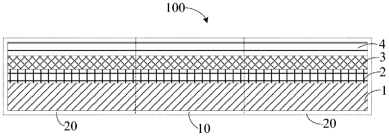
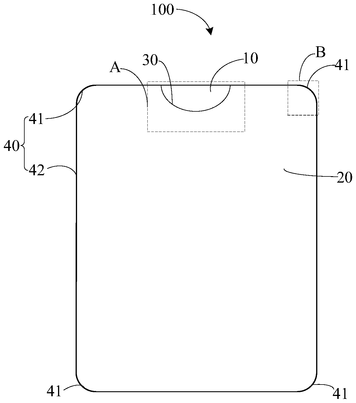
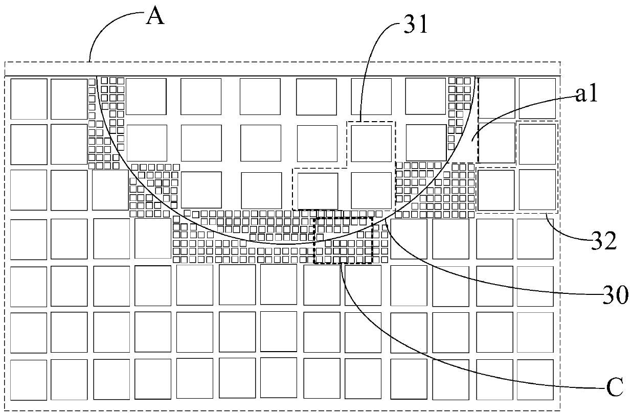
The application provides a display substrate, a display panel and a display device. The display substrate comprises an underlayer, a first electrode layer, a light emitting layer and a second electrode layer, wherein the light emitting layer comprises a plurality of pixel units, and each pixel unit comprises n pixels; the display area comprises a first display area and a second display area with aboundary therebetween, the first display area comprises a plurality of first pixel units, the second display area comprises a plurality of second pixel units, the pixel density of the first display area is smaller than that of the second display area, a first area of the region between each pixel unit of the near boundary in the second display area and the boundary is less than one third of the area of the second pixel units; and / or, the display area has a prepared boundary with at least a part as the non-linear boundary, the pixel units in the display area comprise multiple third pixel units, and the second area of the region between each pixel unit of the adjacent non-linear boundary in the prepared boundary and the non-linear boundary is less than one third of the area of the third pixel units.

Description

technical field [0001] The present application relates to the field of display technology, in particular to a display substrate and a display optimization method thereof, a display panel and a display device. Background technique [0002] With the rapid development of electronic devices, users have higher and higher requirements for screen-to-body ratio, so that the full-screen display of electronic devices has attracted more and more attention from the industry. Traditional electronic devices such as mobile phones, tablet computers, etc., need to integrate such as front camera, earpiece, and infrared sensing components, so it is possible to set the camera, earpiece, and infrared sensing elements in the slotted area by slotting (Notch) on the display screen. Components, etc., but the slotted area cannot be used to display the picture, such as the notch screen in the prior art, or the method of opening holes on the screen. For electronic equipment that realizes the camera fun...

Claims


Application Information

Patent Timeline
IPC IPC(8): H01L27/32G09F9/33
CPCG09F9/33H10K59/352H10K59/60H10K59/353
Inventor 胡凤章王光辉陈峰张金泉
Owner KUNSHAN GO VISIONOX OPTO ELECTRONICS CO LTD
Learn More