Display panel, manufacturing method thereof and display device

A display panel and display area technology, applied in semiconductor/solid-state device manufacturing, semiconductor devices, electrical components, etc., can solve problems such as not being a full screen, achieve high image definition, reduce optical path difference, and avoid short circuits

Active Publication Date: 2020-02-11
KUNSHAN GO VISIONOX OPTO ELECTRONICS CO LTD
View PDF8 Cites 4 Cited by
  • Summary
  • Abstract
  • Description
  • Claims
  • Application Information

AI Technical Summary

Problems solved by technology

However, neither the notch screen nor the perforated screen is a real full

Method used


Image

  • Display panel, manufacturing method thereof and display device
  • Display panel, manufacturing method thereof and display device
  • Display panel, manufacturing method thereof and display device

Examples


Embodiment Construction

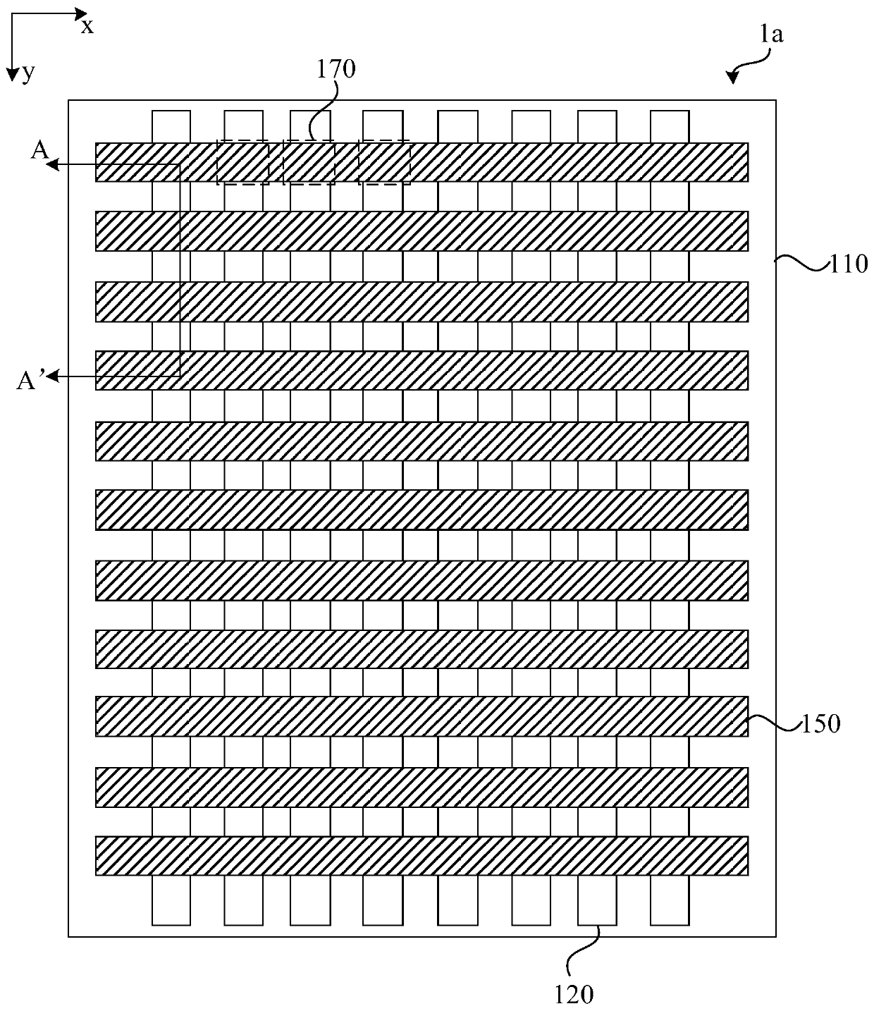
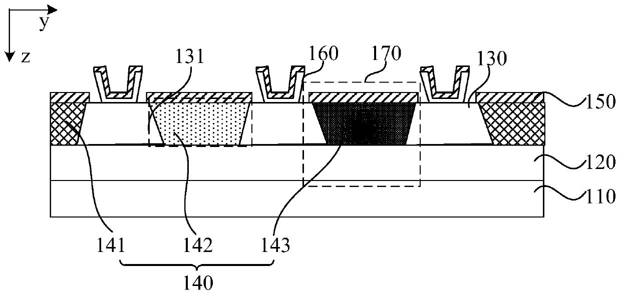
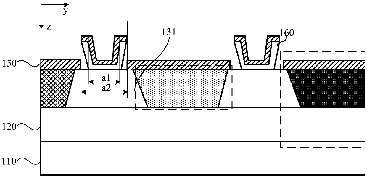
[0059] The present invention will be further described in detail below in conjunction with the accompanying drawings and embodiments. It should be understood that the specific embodiments described here are only used to explain the present invention, but not to limit the present invention. In addition, it should be noted that, for the convenience of description, only some structures related to the present invention are shown in the drawings but not all structures.

[0060] As mentioned in the background technology, no matter whether it is a notch screen or a perforated screen in the prior art, a true full screen cannot be realized. The inventor found through research that to realize a full screen, the display panel needs to be directly covered on the photosensitive device such as the camera, which requires the display panel above the photosensitive device such as the camera to have high light transmittance. However, the inventor further found that, When photosensitive devices...


PUM


Abstract

The embodiment of the invention discloses a display panel, a manufacturing method thereof and a display device. The display panel includes at least a first display area which has a first sub-pixel. The first display area includes a first substrate, a first electrode on one side of the first substrate, and a first pixel-defining layer which is located on one side, which is away from the first substrate, of the first electrode. The first pixel-defining layer includes a first pixel opening which includes a first light-emitting layer, and a second electrode which is located on one side, which is remote from the first substrate, of the first light-emitting layer. The first display area further includes a spacer. The spacer is arranged on one side, which is away from the first substrate, of thefirst pixel-defining layer. The size of the orthogonal projection of the surface of one side, which is away from the first substrate, of the spacer on the first substrate is larger than the size of the orthogonal projection of the surface of one side, which is near the first substrate, of the spacer on the first substrate. A recessed structure is arranged on the surface of one side, which is awayfrom the substrate, of the spacer. The optical path difference of light passing through the spacer can be reduced, thereby reducing the diffraction phenomenon.

Description

technical field [0001] Embodiments of the present invention relate to the field of display technology, and in particular, to a display panel, a manufacturing method thereof, and a display device. Background technique [0002] With the rapid development of display terminals, users have higher and higher requirements for screen-to-body ratio, which makes the full-screen display of display terminals attract more and more attention from the industry. Most of the full-screen displays in the prior art are in the form of slots or openings, such as Liu Haiping, etc., which are slots or openings in the display area corresponding to components such as cameras and sensors. When realizing the camera function, the external light enters the camera below the display screen through the slot or hole on the display screen, so as to realize the photo taking. However, neither the notch screen nor the perforated screen is a true full screen. Therefore, the industry urgently needs to develop a t...

Claims


Application Information

Patent Timeline
IPC IPC(8): H01L51/52H01L51/56H01L27/32
CPCH10K59/351H10K59/17H10K59/122H10K50/86H10K71/00
Inventor 殷汉权吴昊朱可夏宇飞
Owner KUNSHAN GO VISIONOX OPTO ELECTRONICS CO LTD
Why Eureka
Try Eureka