Display panel, manufacturing method thereof and display device

A technology for display panels and display devices, which is applied in the manufacture of semiconductor/solid-state devices, electrical components, and electrical solid-state devices, etc., and can solve the problems of different optical paths and excessively large viewing angle of display panels.

Active Publication Date: 2019-08-23
BOE TECH GRP CO LTD +1
View PDF4 Cites 0 Cited by
  • Summary
  • Abstract
  • Description
  • Claims
  • Application Information

AI Technical Summary

Problems solved by technology

[0005] The present invention provides a display panel, a manufacturing method thereof, and a display device, so as to solve the problem in the prior art that incident light rays with different incident angles have different optical paths in the optical coupling layer, resulting in an excessively large viewing angle of the display panel.

Method used


Image

  • Display panel, manufacturing method thereof and display device
  • Display panel, manufacturing method thereof and display device
  • Display panel, manufacturing method thereof and display device

Examples


Embodiment 1

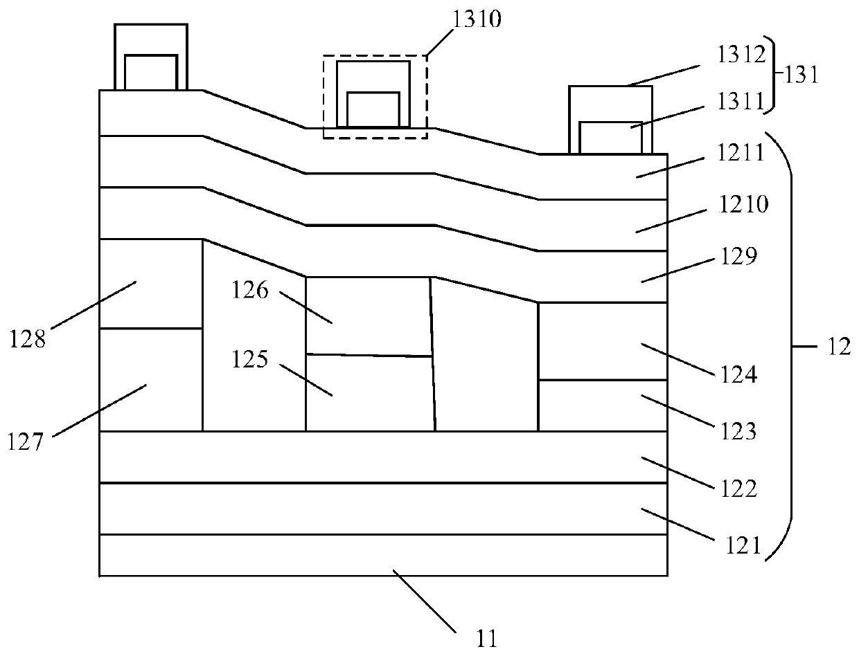
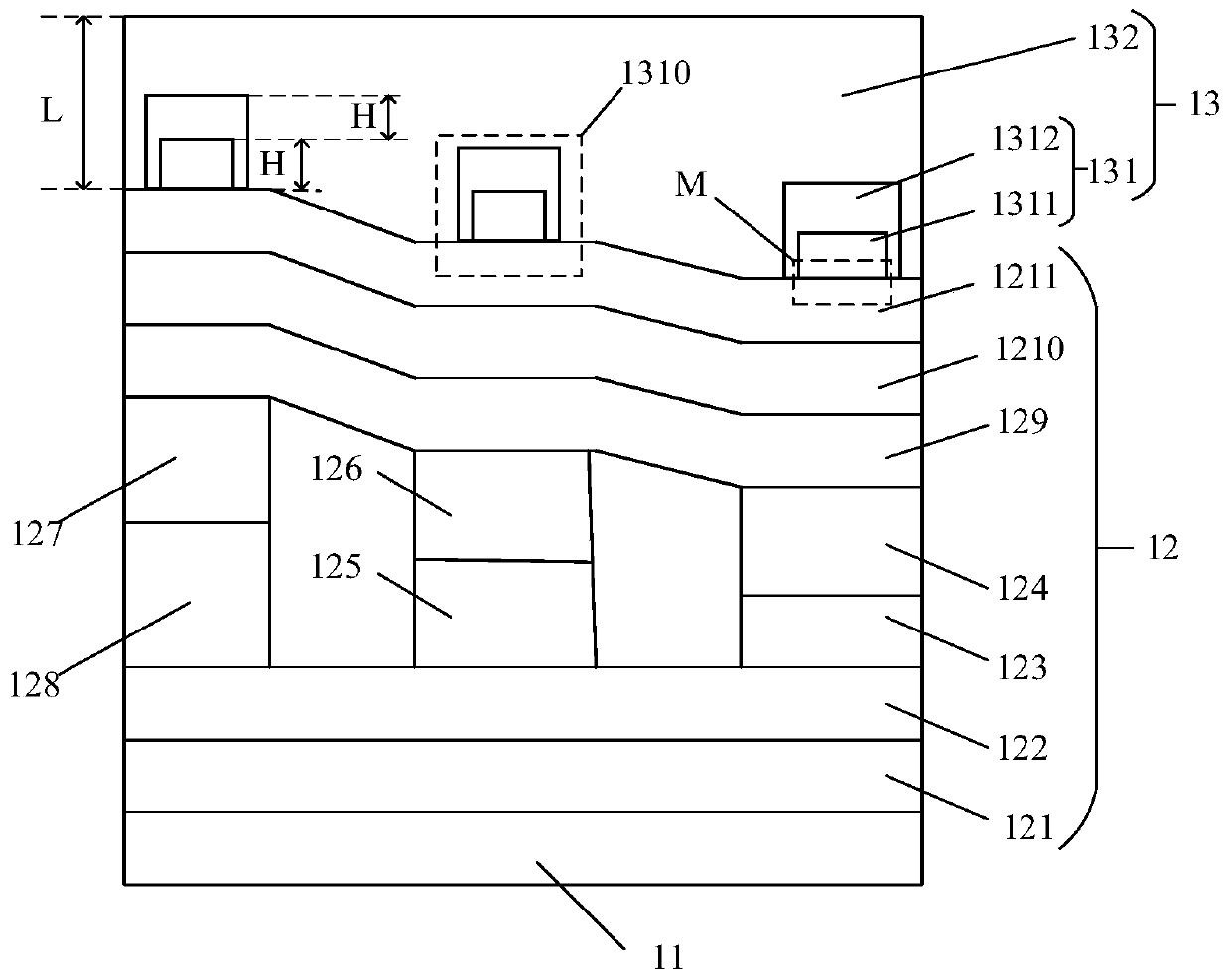
[0038] refer to figure 1 , showing a schematic structural diagram of a display panel according to an embodiment of the present invention, figure 2 A schematic structural diagram of another display panel according to an embodiment of the present invention is shown.

[0039] An embodiment of the present invention provides a display panel, which includes a base substrate 11, a plurality of organic light emitting devices 12 disposed on the base substrate 11, and at least two layers of optical coupling layers 13 disposed on the organic light emitting devices 12 , for any two adjacent optical coupling layers 13, the optical coupling layer 13 far away from the base substrate 11 covers the optical coupling layer 13 close to the base substrate 11, and the refractive index of the optical coupling layer 13 far away from the base substrate 11 is less than The refractive index of the light coupling layer 13 close to the base substrate 11 .

[0040] It should be noted, figure 1 and fi...

Embodiment 2

[0066] refer to Figure 5 , which shows a flow chart of a method for manufacturing a display panel according to an embodiment of the present invention, which may specifically include the following steps:

[0067] Step 501, providing a base substrate.

[0068] Step 502, forming a plurality of organic light emitting devices on the base substrate.

[0069]In the embodiment of the present invention, a plurality of organic light-emitting devices 12 are formed on the base substrate 11. The base substrate 11 may be a glass substrate or a PI (Polyimide, polyimide) substrate. The organic light-emitting devices 12 include The anode 121 on the anode 121, and the hole transport layer 122 arranged on the anode 121, the electron blocking layer arranged on the hole transport layer 122, the color light-emitting layer arranged on the electron block layer, the spacer arranged on the color light-emitting layer A hole blocking layer 129 , an electron transport layer 1210 disposed on the hole bl...

Embodiment 3

[0089] The embodiment of the present invention also discloses a display device, including the above-mentioned display panel. The display panel includes a base substrate 11, a plurality of organic light-emitting devices 12 arranged on the base substrate 11, and a plurality of organic light-emitting devices arranged on the organic light-emitting devices 12. At least two layers of optical coupling layers 13, for any adjacent two layers of optical coupling layers 13, the optical coupling layer 13 away from the base substrate 11 covers the optical coupling layer 13 close to the base substrate 11, and the optical coupling layer 13 away from the base substrate 11 The refractive index of the coupling layer 13 is smaller than that of the optical coupling layer 13 close to the base substrate 11 .

[0090] In this embodiment of the present invention, for a specific description of the display panel, reference may be made to the description of Embodiment 1, which will not be repeated in thi...


PUM


Abstract

The invention provides a display panel, a manufacturing method thereof and a display device, and relates to the technical field of display. The invention provides the display panel. The display panelcomprises a substrate and a plurality of organic light-emitting devices arranged on the substrate, and at least two optical coupling layers which are arranged on the organic light-emitting device. Forany two adjacent optical coupling layers, the optical coupling layer far away from the substrate covers the optical coupling layer close to the substrate, and the refractive index of the optical coupling layer far away from the substrate is less than that of the optical coupling layer close to the substrate. Through at least two optical coupling layers, the display panel enables the wavelength difference of emergent rays to be reduced for light rays at different incident angles, so that the color cast caused by the visual angle is improved.

Description

technical field [0001] The present invention relates to the field of display technology, in particular to a display panel, a manufacturing method thereof, and a display device. Background technique [0002] As display devices are used more and more frequently in people's lives, OLEDs (Organic Light-Emitting Diodes, organic light-emitting diodes) with self-illumination, high contrast, fast response, and bendability have become the current display device industry. popular products, and are widely used in smart watches, mobile phones, TVs and other products. [0003] At present, in the manufacturing process of OLED display panels, the same optical coupling layer material is usually evaporated on the organic light-emitting devices to obtain the optical coupling layer, and the optical coupling layer covers all the organic light-emitting devices in the display panel. [0004] However, since the optical coupling layer covering all organic light-emitting devices is obtained by vapo...

Claims


Application Information

Patent Timeline
Patent Type & Authority Applications(China)
IPC IPC(8): H01L51/52H01L27/32H01L51/56
CPCH10K59/10H10K50/858H10K71/00
Inventor 黄灿史大为赖韦霖鲍建东刘瑞王宇瑶
Owner BOE TECH GRP CO LTD
Why Eureka
Try Eureka