Ink-jet printing method, ink-jet printing device and display device

An inkjet printing device and inkjet printing technology, which are applied in the fields of electrical solid devices, semiconductor devices, semiconductor/solid device manufacturing, etc., can solve the problems of poor film formation, high cost, and inability to produce large-size OLED devices.

Active Publication Date: 2020-02-28
BOE TECH GRP CO LTD
View PDF7 Cites 3 Cited by
  • Summary
  • Abstract
  • Description
  • Claims
  • Application Information

AI Technical Summary

Problems solved by technology

Among them, since the evaporation process requires the use of a mask (Mask), and the mask will fall during the evaporation process, so the film formation effect is not good, and large-size OLED devices cannot be prepared; in addition, the material of the evaporation process Low utilization, leading to high costs
The disadvantages of the evaporation process as mentioned above are just the advantages of inkjet printing technology
However, inkjet printing technology has certain limitations in improving the pixel resolution of OLED display panels, which are mainly reflected in the following aspects: First, the size of the ink drop itself is limited, for example, the diameter of a 1 picoliter (pL) ink drop is usually in the About 13 microns (um), the diameter of a 5pL ink drop is about 21um, and the dia

Method used


Image

  • Ink-jet printing method, ink-jet printing device and display device
  • Ink-jet printing method, ink-jet printing device and display device
  • Ink-jet printing method, ink-jet printing device and display device

Examples


no. 1 example

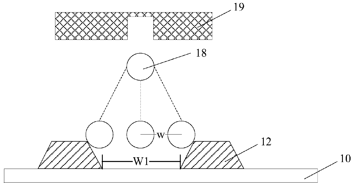
[0035] The inkjet printing method provided in this embodiment includes: spraying ink droplets containing magnetic materials through a nozzle; applying a magnetic force opposite to the direction of gravity to the dropped ink droplets to adjust the shape of the ink droplets.

[0036] In this embodiment, the magnetic material may include at least one of the following: magnetic nanoparticle material, magnetic ionic liquid material. For example, the magnetic material may be a magnetic nanoparticle material, or may be a magnetic ionic liquid material, or may be a combination of a magnetic nanoparticle material and a magnetic ionic liquid material.

[0037] In this embodiment, the particle size of the magnetic nanoparticle material is less than 30 nanometers (nm), and the magnetic nanoparticle material can have superparamagnetic properties, that is, the magnetic hysteresis property disappears, and there is no residual magnetism, so that it will not affect the inkjet printing solution....

no. 2 example

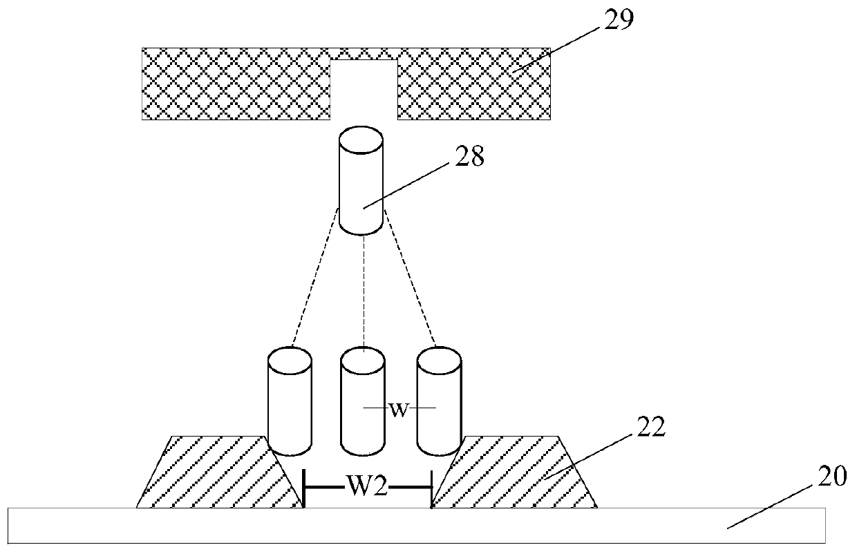
[0044] The inkjet printing method provided in this embodiment includes: spraying ink droplets containing conductive materials through a nozzle; and applying an electric field force opposite to the direction of gravity to the dropped ink droplets to adjust the shape of the ink droplets.

[0045] In an exemplary embodiment, the conductive material may include at least one of the following: colloidal particles adsorbing cations, and colloidal particles adsorbing anions. For example, colloidal particles such as metal hydroxides and metal oxides adsorb cations and are positively charged; colloidal particles such as non-metal oxides and non-metal sulfides adsorb anions and are negatively charged. However, the present application is not limited to this.

[0046] In an exemplary embodiment, the total amount of the conductive material in the ink droplet may be less than 5% of the total amount of the ink droplet, so as to avoid affecting the basic performance of the ink and the prepared...

no. 3 example

[0049] Based on the technical concept of the embodiment of the present application, the embodiment of the present application also provides a display device, including: an anode layer, an organic functional layer and a cathode layer stacked in sequence; wherein, the organic functional layer uses the Prepared by inkjet printing method. Wherein, the organic functional layer may include one or more of the following: a hole injection layer, a hole transport layer, a light emitting layer, an electron transport layer, and an electron injection layer.

[0050] The technical solution of this embodiment will be further described below through the manufacturing process of the display device of this embodiment. Among them, the "patterning process" mentioned in this embodiment includes deposition of film layer, coating of photoresist, mask exposure, development, etching, stripping of photoresist, etc., which is a mature preparation process in related technologies. Deposition can use know...


PUM

PropertyMeasurementUnit
Particle sizeaaaaaaaaaa

Abstract

The invention provides an ink-jet printing method, an ink-jet printing device and a display device. The ink-jet printing method comprises the steps of spraying ink droplets through a sprayer, specifically, the ink droplets comprise at least one of a magnetic material and a conductive material; and applying acting force opposite to the direction of gravity to the dropping ink droplets so as to adjust the shape of the ink droplets.

Description

technical field [0001] This article relates to the field of display technology, especially an inkjet printing method, an inkjet printing device and a display device. Background technique [0002] Organic Light-Emitting Diode (OLED, Organic Light-Emitting Diode) is an electroluminescent device, which has the characteristics of self-luminescence, high luminous efficiency, low operating voltage, light and thin, flexible and simple process technology, and is used in display lighting and other fields. widely. [0003] In the OLED organic light-emitting film layer process, there are mainly dry film-forming process represented by evaporation process and wet film-forming process represented by printing process. Among them, since the evaporation process requires the use of a mask (Mask), and the mask will fall during the evaporation process, so the film formation effect is not good, and large-size OLED devices cannot be prepared; in addition, the material of the evaporation process ...

Claims


Application Information

Patent Timeline
IPC IPC(8): B41J3/407H01L51/56
CPCB41J3/407H10K71/135H10K71/00
Inventor 胡春静侯文军
Owner BOE TECH GRP CO LTD
Why Eureka
Try Eureka