Backlight module, manufacturing method and display device

A technology of backlight module and light-concentrating structure, which is applied in optics, nonlinear optics, character and pattern recognition, etc., and can solve problems such as inability to make through holes

Active Publication Date: 2020-02-28
BOE TECH GRP CO LTD +1
View PDF12 Cites 3 Cited by
  • Summary
  • Abstract
  • Description
  • Claims
  • Application Information

AI Technical Summary

Problems solved by technology

However, at present, Mini LEDs are mostly driven by PCB substrates, and it is impossible to make through holes to continue integrating devices under Mini LEDs.

Method used


Image

  • Backlight module, manufacturing method and display device
  • Backlight module, manufacturing method and display device
  • Backlight module, manufacturing method and display device

Examples


Embodiment Construction

[0062] In order to illustrate the present invention more clearly, the present invention will be further described below in conjunction with preferred embodiments and accompanying drawings. Similar parts in the figures are denoted by the same reference numerals. Those skilled in the art should understand that the content specifically described below is illustrative rather than restrictive, and should not limit the protection scope of the present invention.

[0063]It should be noted that "on", "formed on" and "arranged on" mentioned in this article may mean that one layer is directly formed or set on another layer, or that a A layer is indirectly formed or disposed on another layer, ie there are other layers between the two layers. In this document, unless otherwise specified, the term "on the same layer" used means that two layers, parts, members, elements or parts can be formed by the same patterning process, and that the two layers, parts, members, Elements or parts are ge...


PUM


Abstract

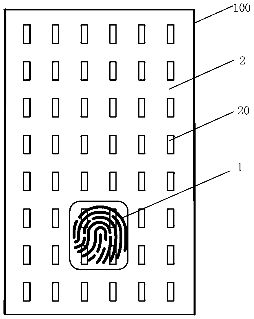
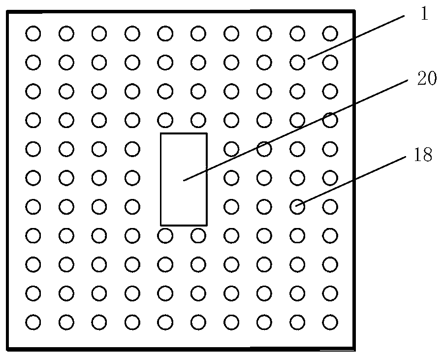
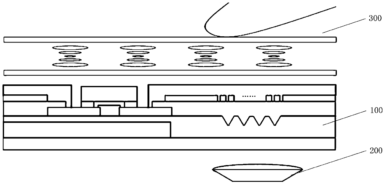
The invention discloses a backlight module, a manufacturing method and a display device. The backlight module comprises a fingerprint acquisition area and a non-fingerprint acquisition area, and the non-fingerprint acquisition area is provided with a first Mini LED array; the fingerprint acquisition area is provided with a second Mini LED array and acquisition holes surrounding Mini LED lamp beadsin the second Mini LED array, and the acquisition holes are used for transmitting light emitted by the backlight module and reflected by a fingerprint to be detected to a fingerprint collector. According to the embodiment provided by the invention, the light reflected by the fingerprint to be detected is transmitted through the acquisition holes formed in the fingerprint acquisition area of the backlight module, and therefore, the fingerprint collector arranged at the rear end of the backlight module can carry out fingerprint identification according to the reflected light, fingerprint identification under the screen of the liquid crystal display device of the backlight module based on the Mini LED is achieved, and the backlight module has wide application prospects.

Description

technical field [0001] The invention relates to the field of display technology, in particular to a backlight module, a manufacturing method and a display device. Background technique [0002] In order to increase the screen-to-body ratio of the display screen of the mobile phone panel, an under-screen fingerprint recognition technology is proposed. Currently, under-screen fingerprints are mostly used on AMOLED display panels. Traditional LCDs cannot use the corresponding technology of AMOLED display panels because the backlight is the entire surface. However, as the market demand for high dynamic range image (HDR) display increases, liquid crystal LCD display panels can realize HDR display by using Mini LED backlight modules instead of traditional backlight modules. However, at present, Mini LEDs are mostly driven by PCB substrates, and it is impossible to make through holes to continue integrating devices under Mini LEDs. Contents of the invention [0003] In order to ...

Claims


Application Information

Patent Timeline
Patent Type & Authority Applications(China)
IPC IPC(8): G02F1/13357G02F1/1333G06K9/00
CPCG02F1/133603G02F1/133605G02F1/13338G02F1/133612G06V40/1318
Inventor 方浩博张勇王建华刚林坚张丽敏杨智超秦相磊孙泽鹏
Owner BOE TECH GRP CO LTD
Why Eureka
Try Eureka