Touch structure, touch method and touch display device
A technology of touch and touch electrodes, which is applied in the field of touch display devices and can solve problems such as cumbersome operations
- Summary
- Abstract
- Description
- Claims
- Application Information
AI Technical Summary
Problems solved by technology
Method used
Image
Examples
Embodiment 1
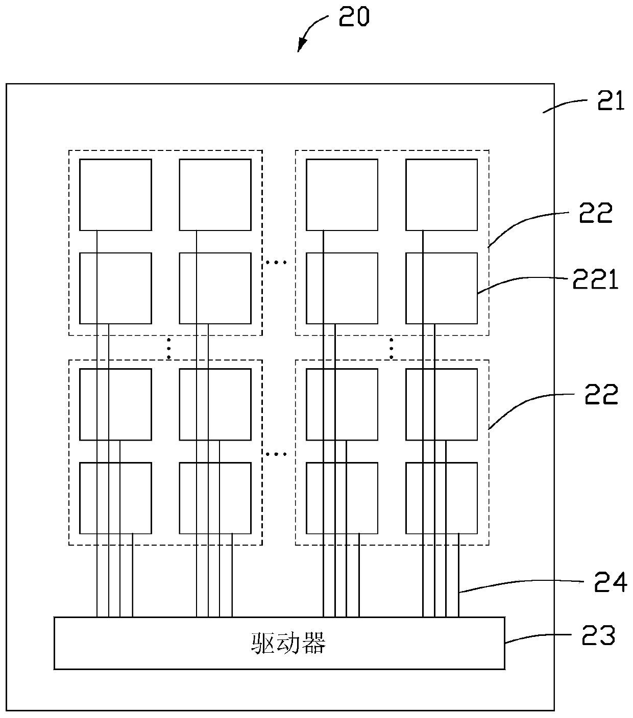
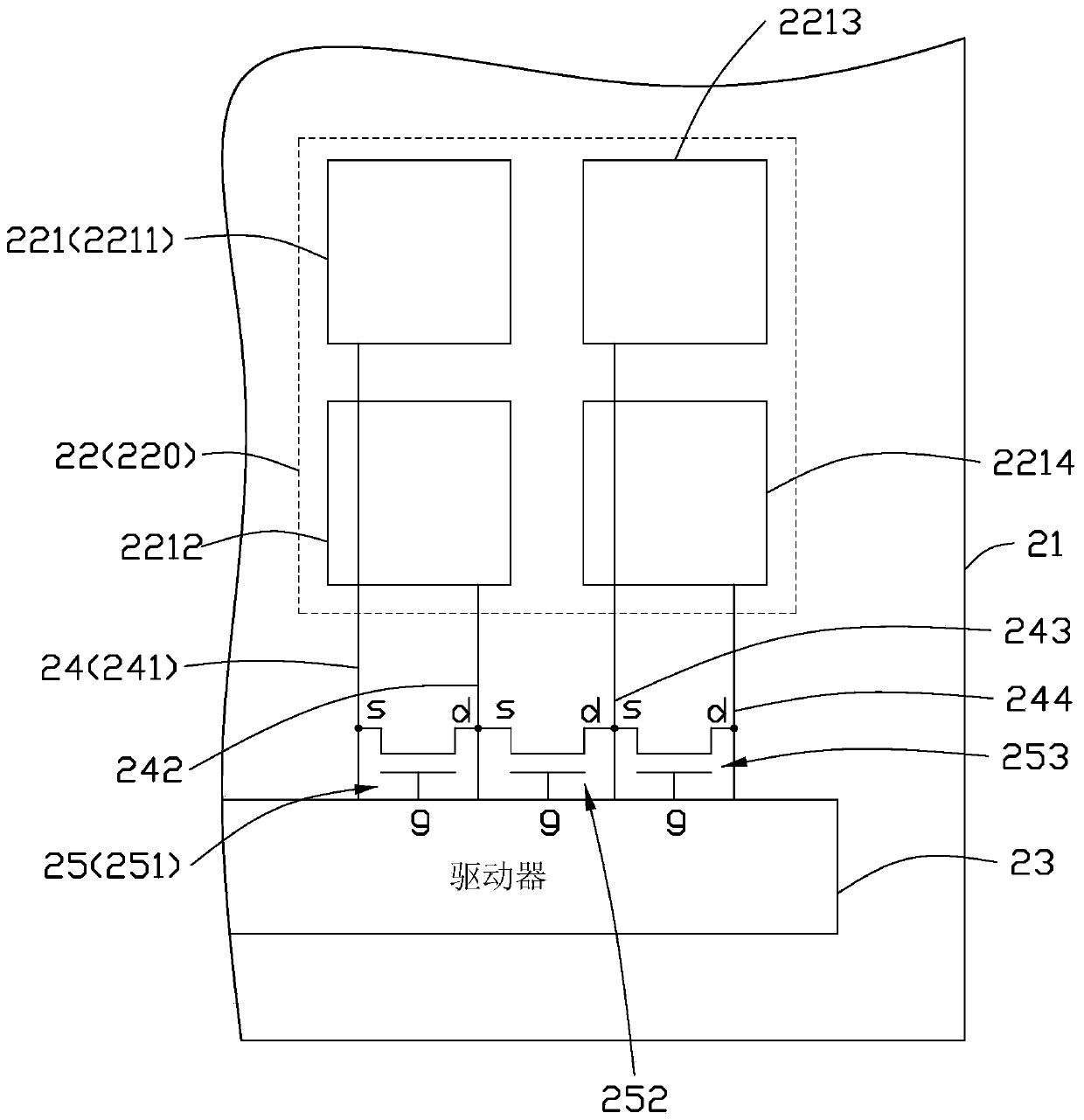
[0035] see figure 1 , the touch display device 10 provided in this embodiment includes a touch structure 20 , a display panel 30 and a cover plate 40 . Wherein, in this embodiment, the touch structure 20 is stacked with the display panel 30 as a structure independent of the display panel 30 , and the cover plate 40 is covered on the side of the touch structure 20 away from the display panel 30 . In other embodiments, the touch structure 20 can be embedded in the display panel 30 , and the embodiment of the present invention does not limit the structure of the touch structure 20 and the display panel 30 . The touch structure 20 is used to identify the user's touch operation on the touch structure 20, the display panel 30 is used to display images according to the touch operation, the surface 41 of the cover plate 40 is used to display the image displayed on the display panel 30, It is also used to receive the user's touch operation. In this embodiment, the user's touch operat...
Embodiment 2
[0066] Please refer to 10, the difference between the touch control structure 50 provided in this embodiment and the first embodiment is that the first switch element 25 is replaced by the second switch element 55 in this embodiment.
[0067] read on Figure 10 In the touch structure 50 provided in this embodiment, in each touch unit 52, a second switch element 55 is electrically connected between every two adjacent touch electrodes 521. In this embodiment, the second switch element 55 It is a thin film transistor and is arranged on the substrate 51 . The gate g of the second switch element 55 is electrically connected to the driver 53 , and the source s and the drain d are respectively electrically connected to a touch electrode 521 . According to the operating characteristics of the thin film transistor, when the voltage applied to the gate g of the second switching element 55 reaches the threshold voltage of the second switching element 55, the source s and the drain d of ...
PUM
 Abstract
Description
Claims
Application Information


